Applied Materials Centura RP
Introduction to Centura RP
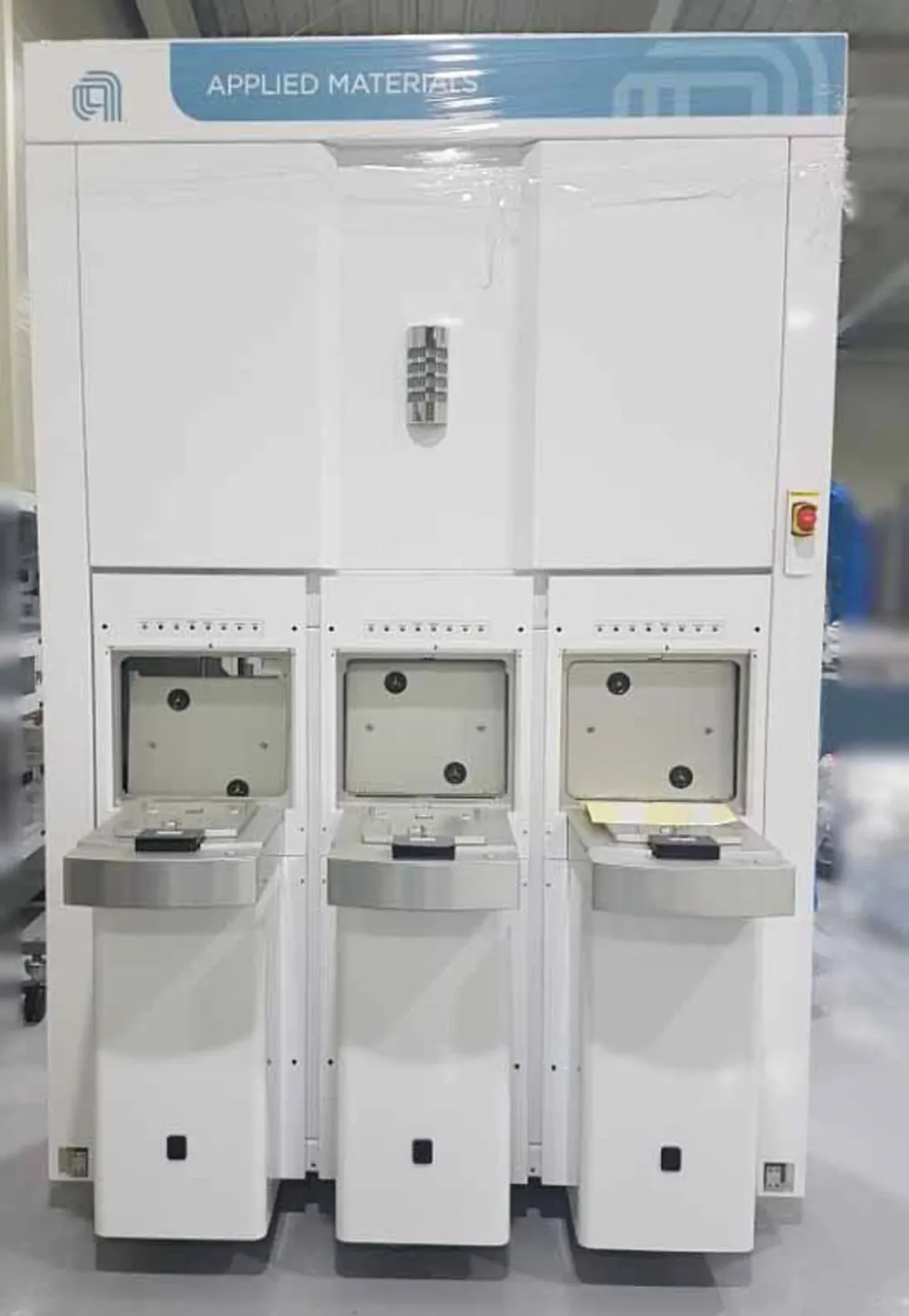
The Applied Materials Centura RP is a production-ready epitaxial deposition platform that enables void-free gate-all-around (GAA) transistor's source-drain structures through continuous etch-deposition control. This system is designed to address the challenges of etching and epitaxial growth in high aspect ratio environments, which are critical for the development of next-generation logic and memory devices. The Centura RP system is optimized for emerging applications of epitaxial films, enabling faster transistor switching speed without the need to shrink the scale of the device.Key Features and Specifications
The Centura RP system features a range of advanced technologies, including:Performance and Benefits
The Centura RP system offers a range of benefits, including: * High-productivity etch and epitaxial growth capabilities * Advanced uniformity control for optimal etch and epitaxial growth performance * Reduced gas consumption through advanced process control and optimization * Enable faster transistor switching speed without the need to shrink the scale of the device * Compatible with a range of semiconductor materials and processes
What is the Centura RP system used for?
The Centura RP system is used for high-productivity silicon, metal, and dielectric etch, as well as precision epitaxial growth of silicon, silicon-germanium, and other materials.
What are the key features of the Centura RP system?The Centura RP system features advanced etch and epitaxial growth technologies, including plasma etching of silicon dioxide, silicon nitride, and other materials, and precision epitaxial growth of silicon, silicon-germanium, and other materials.
What are the benefits of using the Centura RP system?The Centura RP system offers a range of benefits, including high-productivity etch and epitaxial growth capabilities, advanced uniformity control, reduced gas consumption, and enable faster transistor switching speed without the need to shrink the scale of the device.
Specifications
| Specification | Description |
|---|---|
| Etch Technology | Plasma etching of silicon dioxide, silicon nitride, and other materials |
| Epitaxial Growth | Precision epitaxial growth of silicon, silicon-germanium, and other materials |
| Aspect Ratio | High aspect ratio etch and epitaxial growth capabilities |
| Throughput | High-productivity etch and epitaxial growth capabilities |
| Uniformity | Advanced uniformity control for optimal etch and epitaxial growth performance |
| Gas Consumption | Reduced gas consumption through advanced process control and optimization |
| Transistor Switching Speed | Enable faster transistor switching speed without the need to shrink the scale of the device |
| Compatibility | Compatible with a range of semiconductor materials and processes |