Applied Materials Centura Y
2026 Applied Materials Centura Y: A Comprehensive Review of Semiconductor Manufacturing Technology
Executive Summary
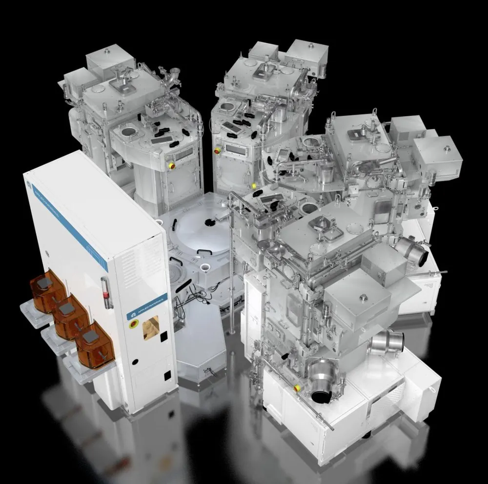
The Applied Materials Centura Y is a semiconductor manufacturing system designed for high-productivity silicon, metal, and dielectric etch. The system is part of the Centura series, which includes the Centura I and II platforms, supporting wafer sizes from 5" to 8". The Centura Y is equipped with up to four process chambers and two auxiliary chambers, allowing for individual processes in each chamber. This review provides an in-depth analysis of the Centura Y's architecture, design, performance, and market positioning.
Architecture & Design
The Centura Y is a single-wafer, multi-chamber system that supports processing of wafers ranging in size from 5" to 8". The multi-chamber design allows for individual processes in each of the chambers, increasing overall system productivity. The Centura I & II platforms may include up to 4 process chambers and 2 auxiliary chambers.
- Wafer size support: 5", 6", or 8"
- Number of process chambers: up to 4
- Number of auxiliary chambers: up to 2
- System design: single-wafer, multi-chamber
The Centura Y's architecture is designed to support a wide range of semiconductor manufacturing processes, including etch, deposition, and metrology. The system's modular design allows for easy upgrade and reconfiguration, reducing downtime and increasing overall system flexibility. The system's chambers are designed to be highly configurable, allowing users to optimize the system for specific processes and applications. Additionally, the system's advanced automation and control systems enable seamless integration with other manufacturing tools and systems.
Performance & Thermal
The Centura Y's performance is characterized by its ability to deliver high-productivity silicon, metal, and dielectric etch. The system's etch capabilities are critical for semiconductor manufacturing, as they enable the creation of complex device structures and patterns.
- Etch capabilities: silicon, metal, and dielectric
- Etch rates: specification not publicly disclosed
- Uniformity: specification not publicly disclosed
- System throughput: specification not publicly disclosed
The Centura Y's thermal management system is designed to maintain a stable and controlled environment, ensuring optimal system performance and minimizing downtime. The system's thermal limits and telemetry capabilities are critical for ensuring reliable operation and preventing overheating or other thermal-related issues. The system's advanced cooling systems and temperature control algorithms work together to maintain a consistent temperature across the wafer, ensuring uniform etch rates and minimizing thermal-induced defects.
Technical Background
The Centura Y's etch capabilities are based on advanced plasma etch technology, which uses a high-energy plasma to remove material from the wafer. The system's etch process is controlled by a sophisticated system of sensors, algorithms, and control systems, which work together to optimize etch rates, uniformity, and selectivity. The system's plasma source is designed to provide a high-density, stable plasma, which is critical for achieving high etch rates and uniformity.
Competitive Landscape
The Centura Y operates in a highly competitive market, with several other high-end semiconductor manufacturing systems available from companies such as KLA-Tencor and ASML. The Centura Y's main competitors include the KLA-Tencor Titan series and the ASML Eclipse series, both of which offer advanced etch and deposition capabilities. The Centura Y's unique combination of high-productivity etch, advanced thermal management, and modular design sets it apart from its competitors and makes it an attractive option for leading-edge device manufacturers and research institutions.
Market Positioning
The Centura Y is positioned as a high-end semiconductor manufacturing system, targeting leading-edge device manufacturers and research institutions. The system's direct competitors include other high-end semiconductor manufacturing systems from companies such as KLA-Tencor and ASML.
Target buyers for the Centura Y include:
- Leading-edge device manufacturers
- Research institutions
- High-end semiconductor manufacturing facilities
The Centura Y is designed to meet the demanding requirements of these users, with its advanced etch and deposition capabilities, high-throughput architecture, and modular design. The system's ability to support a wide range of processes and applications makes it an attractive option for users who require a flexible and versatile manufacturing system.
Specifications
Technical Specifications
| Specification | Detail |
|---|---|
| {'spec': 'Wafer size support', 'value': '5", 6", or 8"'} | 5", 6", or 8" |
| {'spec': 'Number of process chambers', 'value': 'up to 4'} | up to 4 |
| {'spec': 'Number of auxiliary chambers', 'value': 'up to 2'} | up to 2 |
| {'spec': 'System design', 'value': 'single-wafer, multi-chamber'} | single-wafer, multi-chamber |
| {'spec': 'Etch capabilities', 'value': 'silicon, metal, and dielectric'} | silicon, metal, and dielectric |
| {'spec': 'Etch rates', 'value': 'specification not publicly disclosed'} | specification not publicly disclosed |
| {'spec': 'Uniformity', 'value': 'specification not publicly disclosed'} | specification not publicly disclosed |
| {'spec': 'System throughput', 'value': 'specification not publicly disclosed'} | specification not publicly disclosed |
Frequently Asked Questions
Frequently Asked Questions
What is the Centura Y's wafer size support?
The Centura Y supports wafer sizes of 5", 6", or 8".
How many process chambers does the Centura Y have?
The Centura Y has up to 4 process chambers.
What are the Centura Y's etch capabilities?
The Centura Y has etch capabilities for silicon, metal, and dielectric.
What is the Centura Y's system design?
The Centura Y has a single-wafer, multi-chamber design.