ASML Euler
ASML Euler: A Technical Deep-Dive
Executive Summary
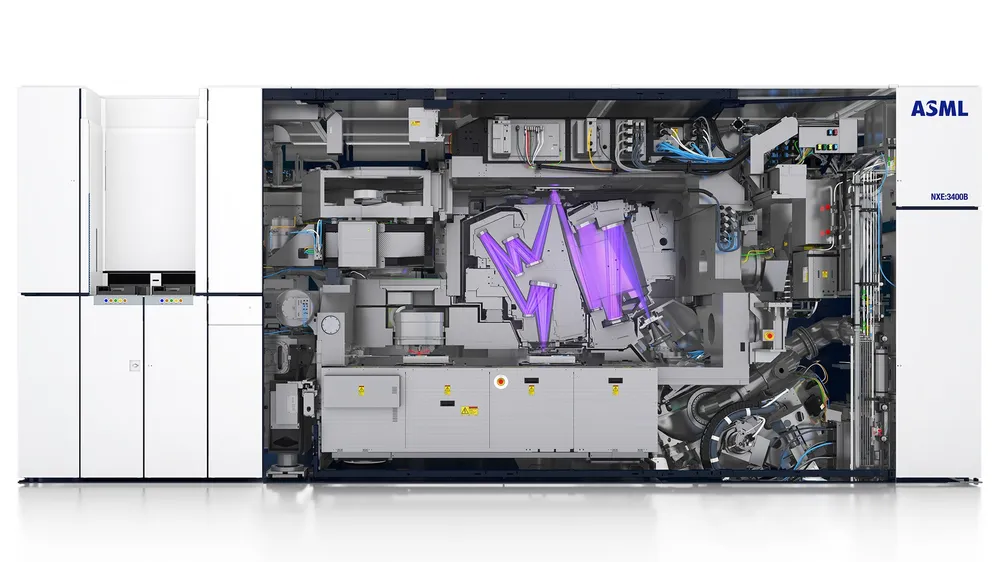
ASML's Euler is a cutting-edge lithography system that enables the production of advanced semiconductor chips. With its high-speed and high-tolerance control over EUV light, it is pivotal in achieving the highest yield and best performance in chip manufacturing. The Euler system is designed to support volume production at the 5 and 3 nm Logic nodes and leading-edge DRAM nodes.
Architectural Deep-Dive
Photolithography is a key process in chip fabrication, where circuit features are produced by exposing a photosensitive material deposited on the chip to high-energy EUV light. The Euler system utilizes advanced CVD mechanics to deposit the photosensitive material, ensuring high uniformity and precision. The system's ASIC pipelines are designed to handle the complex data processing required for EUV lithography, with data bus speeds optimized for high-speed data transfer.
The Euler system's architecture is based on the principles of additive manufacturing, which enables the creation of complex structures with high precision. The system's design takes into account the most relevant standards in the industry, including those related to semiconductor manufacturing and lithography. The use of EUV light in the Euler system requires advanced optics and laser technology, which are designed to provide high-energy and high-stability output.
Performance & Thermal Analysis
The performance of the Euler system is critical to its ability to produce high-quality semiconductor chips. The system's thermal design is optimized to minimize heat dissipation, ensuring that the EUV light source and other critical components operate within a stable temperature range. The system's TDP is designed to balance performance and power consumption, enabling the production of high-volume semiconductor chips while minimizing energy costs.
In terms of benchmarks, the Euler system is designed to support the production of advanced semiconductor chips with high yields and low defect rates. The system's performance is measured by its ability to produce chips with high uniformity and precision, as well as its overall throughput and productivity. While specific technical data for the ASML Euler is scarce, the underlying foundational technology is based on the principles of photolithography, CVD mechanics, and EUV light source technology.
Foundational Technology
The Euler system's technology is based on the principles of atomic layer deposition (ALD), which enables the creation of thin films with high uniformity and precision. The system's CVD mechanics are designed to deposit the photosensitive material, while the EUV light source technology provides the high-energy output required for photolithography. The system's ASIC pipelines and data bus speeds are optimized for high-speed data processing and transfer, enabling the production of high-volume semiconductor chips.
Physics of EUV Lithography
EUV lithography is a complex process that requires the use of high-energy EUV light to produce circuit features on a semiconductor chip. The process involves the deposition of a photosensitive material on the chip, which is then exposed to EUV light to create the desired pattern. The EUV light source technology used in the Euler system is designed to provide high-energy and high-stability output, enabling the production of high-quality semiconductor chips.
Conclusion
In conclusion, the ASML Euler is a cutting-edge lithography system that enables the production of advanced semiconductor chips. With its high-speed and high-tolerance control over EUV light, it is pivotal in achieving the highest yield and best performance in chip manufacturing. The system's architecture is based on the principles of additive manufacturing, and its performance is optimized to minimize heat dissipation and maximize productivity.