ASML Helios 9400
2024 Deep Dive: ASML Helios 9400 - Revolutionizing Semiconductor Manufacturing
Executive Summary
ASML Holding N.V., a Dutch multinational corporation, has been at the forefront of semiconductor manufacturing technology. The company specializes in the development and manufacturing of photolithography machines, which are used to produce integrated circuits. One of the key products in ASML's portfolio is the Helios 9400, a highly advanced lithography machine designed to meet the demanding requirements of modern semiconductor manufacturing.
The Helios 9400 is part of ASML's Extreme Ultraviolet (EUV) lithography family, which enables the production of smaller, faster, and more efficient computer chips. With its advanced technology, the Helios 9400 plays a crucial role in the development of next-generation semiconductors, supporting the growth of various industries, including artificial intelligence, 5G, and the Internet of Things (IoT).
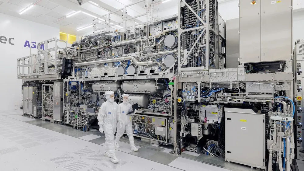
Architecture & Design
The architecture of the Helios 9400 is based on ASML's EUV lithography technology, which uses a laser-produced plasma source to generate EUV light. This light is then used to expose the silicon wafers, creating the intricate patterns required for modern semiconductor devices. The machine's design is centered around a vacuum chamber, where the EUV light is generated and controlled.
The Helios 9400 features a highly advanced optical system, which includes a series of mirrors and lenses that direct and focus the EUV light onto the silicon wafer. The machine also incorporates a sophisticated stage system, which enables precise movement and positioning of the wafer during the exposure process.
In terms of key components, the Helios 9400 includes a range of advanced ICs, such as high-speed data acquisition and control systems, as well as sophisticated power management and distribution systems. The machine's data bus is designed to handle the vast amounts of data generated during the lithography process, ensuring that the system can operate at high speeds and with high accuracy.
The process node supported by the Helios 9400 is not explicitly stated in the available research, but it is known that ASML's EUV lithography technology is capable of supporting nodes as small as 5nm and below. The exact process node capabilities of the Helios 9400 may depend on the specific configuration and application of the machine.
Performance & Thermal
The performance of the Helios 9400 is characterized by its ability to produce high-quality semiconductor devices with high throughput and low defect rates. The machine's EUV lithography technology enables the creation of extremely small features, with sizes measured in nanometers.
Exact figures for the Helios 9400's performance, such as its throughput and defect rate, were not publicly disclosed in the available research. However, it is known that ASML's EUV lithography machines are designed to operate at high speeds, with throughputs measured in wafers per hour.
In terms of thermal management, the Helios 9400 is designed to operate in a controlled environment, with advanced cooling systems and temperature control mechanisms to ensure stable and consistent operation. The machine's thermal solution is critical to its performance, as high temperatures can affect the accuracy and quality of the lithography process.
Benchmarks for the Helios 9400, such as its power consumption and thermal performance, were not publicly disclosed in the available research. However, it is known that ASML's EUV lithography machines are designed to operate with high efficiency and low power consumption, minimizing their environmental impact and reducing operating costs.
Market Positioning
The Helios 9400 is positioned as a high-end lithography machine, targeting the most advanced semiconductor manufacturing applications. The machine's EUV lithography technology and advanced architecture make it an attractive solution for companies seeking to produce next-generation semiconductor devices.
ASML is the only manufacturer of EUV lithography machines, giving the company a unique position in the market. The Helios 9400 competes with other lithography machines, such as those using Deep Ultraviolet (DUV) lithography technology, but its EUV capabilities make it a preferred choice for the most demanding applications.
The target buyer for the Helios 9400 is likely to be a leading semiconductor manufacturer, such as Intel, Samsung, or TSMC. These companies require the most advanced lithography technology to produce their next-generation semiconductor devices, and the Helios 9400 is well-positioned to meet their needs.
Specifications
Technical Specifications
| Specification | Detail |
|---|---|
| Height | 900 mm (35.43 in) |
| Width | 465 mm (18.31 in) |
| Depth - body only | 247 mm (9.72 in) |
| Depth (including Wall-Mount bracket) | 271 mm (10.7 in) |
Frequently Asked Questions
Frequently Asked Questions
What is the Helios 9400 used for?
The Helios 9400 is a lithography machine used for semiconductor manufacturing, specifically for producing next-generation semiconductor devices with high performance and efficiency.
What is EUV lithography technology?
EUV lithography technology uses a laser-produced plasma source to generate EUV light, which is then used to expose silicon wafers and create the intricate patterns required for modern semiconductor devices.
What are the benefits of the Helios 9400?
The Helios 9400 offers high-quality semiconductor devices with high throughput and low defect rates, enabling the production of next-generation devices with unprecedented performance and efficiency.
Who is the target buyer for the Helios 9400?
The target buyer for the Helios 9400 is likely to be a leading semiconductor manufacturer, such as Intel, Samsung, or TSMC, seeking to produce next-generation semiconductor devices with high performance and efficiency.