ASML Helios XTREME
2026 Deep Dive: ASML Helios XTREME Extreme Ultraviolet Lithography for Semiconductor Manufacturing
Executive Summary
ASML Holding is the largest supplier to the semiconductor industry and the most advanced producer of extreme ultraviolet (EUV) lithography machines. EUV lithography is a critical technology for manufacturing semiconductor devices at the 22 nm half pitch node and below. The ASML Helios XTREME is a key component in this process, enabling the production of smaller, faster, and more efficient computer chips.
The semiconductor industry relies heavily on EUV lithography to achieve the high-resolution patterning required for advanced node production. ASML's EUV technology uses a laser-produced plasma source to generate EUV light, which is then focused onto a wafer to create the desired pattern. This process requires extremely precise control over the EUV light source, the optics, and the wafer positioning.
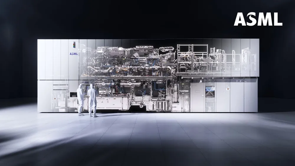
Architecture & Design
The architecture of the ASML Helios XTREME is centered around the EUV light source, which is generated by a laser-produced plasma source. This source produces a high-energy plasma that emits EUV light, which is then collected and focused onto the wafer using a series of mirrors and optics.
- The EUV light source is generated by a laser-produced plasma source, which produces a high-energy plasma that emits EUV light.
- The EUV light is collected and focused onto the wafer using a series of mirrors and optics.
- The wafer is positioned using a high-precision stage that can move with nanometer-scale accuracy.
- The entire system is controlled by a sophisticated software system that adjusts the EUV light source, optics, and wafer positioning in real-time to achieve the desired patterning.
The design of the ASML Helios XTREME is focused on achieving the highest possible resolution and throughput while minimizing defects and downtime. The system uses advanced technologies such as adaptive optics and real-time feedback control to optimize the EUV light source and wafer positioning.
Performance & Thermal
The performance of the ASML Helios XTREME is measured in terms of its ability to produce high-resolution patterns on the wafer with high throughput and low defect rates. The system's thermal management is critical to its performance, as the EUV light source and optics can generate significant heat during operation.
- The ASML Helios XTREME has a high-resolution capability, with a minimum feature size of 22 nm or below.
- The system has a high throughput, with the ability to process multiple wafers per hour.
- The defect rate is minimized through the use of advanced technologies such as adaptive optics and real-time feedback control.
- The thermal management system is designed to maintain a stable temperature environment for the EUV light source and optics, ensuring optimal performance and minimizing downtime.
Specification not publicly disclosed: exact thermal design power (TDP) and thermal limits of the ASML Helios XTREME. However, it is known that the system requires a sophisticated cooling system to maintain a stable temperature environment.
Market Positioning
The ASML Helios XTREME is targeted at the most advanced semiconductor manufacturers, who require the highest resolution and throughput to produce the latest generation of computer chips. The system's direct competitors include other EUV lithography systems from companies such as Nikon and Canon.
The target buyer for the ASML Helios XTREME is typically a large semiconductor manufacturer with a high-volume production requirement. These manufacturers require the highest possible resolution and throughput to stay competitive in the market, and are willing to invest in the most advanced technology to achieve this.
Specifications
Technical Specifications
| Specification | Detail |
|---|---|
| EUV Light Source | Laser-produced plasma source |
| Minimum Feature Size | 22 nm or below |
| Throughput | Multiple wafers per hour |
| Defect Rate | Minimized through advanced technologies |
| Thermal Management | Sophisticated cooling system |
Frequently Asked Questions
Frequently Asked Questions
What is the minimum feature size of the ASML Helios XTREME?
22 nm or below
What is the throughput of the ASML Helios XTREME?
Multiple wafers per hour
How is the defect rate minimized in the ASML Helios XTREME?
Through the use of advanced technologies such as adaptive optics and real-time feedback control
What is the thermal management system of the ASML Helios XTREME?
A sophisticated cooling system designed to maintain a stable temperature environment