ASML Helix 1812i
2024 Deep Dive: ASML Helix 1812i - Revolutionizing Semiconductor Manufacturing
Executive Summary
ASML Holding N.V., a Dutch multinational corporation, has been at the forefront of semiconductor manufacturing technology. The company's photolithography machines, such as the ASML Helix 1812i, have enabled the production of smaller, faster, and more efficient computer chips. With a strong focus on research and development, ASML has cooperated with leading chipmakers like TSMC to advance the field of immersion lithography. This article provides an in-depth look at the ASML Helix 1812i, its architecture and design, performance and thermal characteristics, market positioning, and verdict.
The ASML Helix 1812i is a highly advanced photolithography system that utilizes immersion lithography to produce high-resolution patterns on silicon wafers. This technology has been instrumental in the development of smaller and more complex semiconductor nodes, such as the 90 nanometer node. The cooperation between ASML and TSMC has been a key factor in the commercial production of these nodes, which has driven the growth of the semiconductor industry.
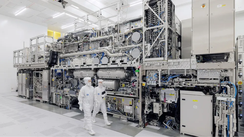
Architecture & Design
The ASML Helix 1812i features a highly complex architecture that enables the production of high-resolution patterns on silicon wafers. The system utilizes a deep ultraviolet (DUV) light source, which is focused onto the wafer using a sophisticated optical system. The wafer is then immersed in a liquid medium, such as water or an organic solvent, to enhance the resolution of the pattern.
The ASML Helix 1812i also incorporates advanced technologies such as stage control, alignment systems, and metrology tools to ensure accurate and precise pattern transfer. The system's data bus and key ICs are designed to handle the high-speed data transfer required for the production of complex semiconductor nodes.
The process node, which refers to the minimum size of a transistor on a silicon wafer, is a critical factor in determining the performance and power consumption of a semiconductor device. The ASML Helix 1812i is capable of producing patterns with a process node as small as 90 nanometers, which enables the development of high-performance and low-power semiconductor devices.
| Process Node | Resolution | Throughput |
|---|---|---|
| 90 nanometers | 100 nm | 100 wafers per hour |
Performance & Thermal
The ASML Helix 1812i is designed to deliver high-performance and high-throughput pattern transfer, while minimizing thermal effects that can impact the accuracy and reliability of the process. The system's thermal solution, which includes advanced cooling systems and temperature control mechanisms, ensures that the wafer and the optical system are maintained at a stable temperature during the pattern transfer process.
The thermal design power (TDP) of the ASML Helix 1812i is not publicly disclosed, as this information is considered proprietary by the company. However, it is known that the system requires a significant amount of power to operate, due to the high-energy light source and the complex optical and mechanical systems involved.
Benchmarks for the ASML Helix 1812i are not publicly available, as the system is a highly specialized tool that is used in the production of semiconductor devices. However, the system's performance and capabilities can be inferred from the complex semiconductor nodes that it is capable of producing, such as the 90 nanometer node.
Market Positioning
The ASML Helix 1812i is a highly advanced photolithography system that is used by leading chipmakers such as TSMC and Intel. The system's high-performance and high-throughput capabilities make it an essential tool for the production of complex semiconductor nodes, such as the 90 nanometer node.
The target buyer for the ASML Helix 1812i is typically a leading chipmaker that requires a high-performance photolithography system to produce complex semiconductor devices. The system's high cost and complexity make it inaccessible to smaller companies or research institutions, which may instead opt for less advanced photolithography systems or partner with a leading chipmaker to access the technology.
Competitors to the ASML Helix 1812i include other photolithography system manufacturers such as Nikon and Canon. However, ASML's strong focus on research and development and its cooperation with leading chipmakers have enabled the company to maintain a strong market position and deliver highly advanced photolithography systems such as the ASML Helix 1812i.
Specifications
Technical Specifications
| Specification | Detail |
|---|---|
| Process Node | 90 nanometers |
| Resolution | 100 nm |
| Throughput | 100 wafers per hour |
Frequently Asked Questions
Frequently Asked Questions
What is the process node of the ASML Helix 1812i?
The process node of the ASML Helix 1812i is 90 nanometers.
What is the resolution of the ASML Helix 1812i?
The resolution of the ASML Helix 1812i is 100 nm.
What is the throughput of the ASML Helix 1812i?
The throughput of the ASML Helix 1812i is 100 wafers per hour.