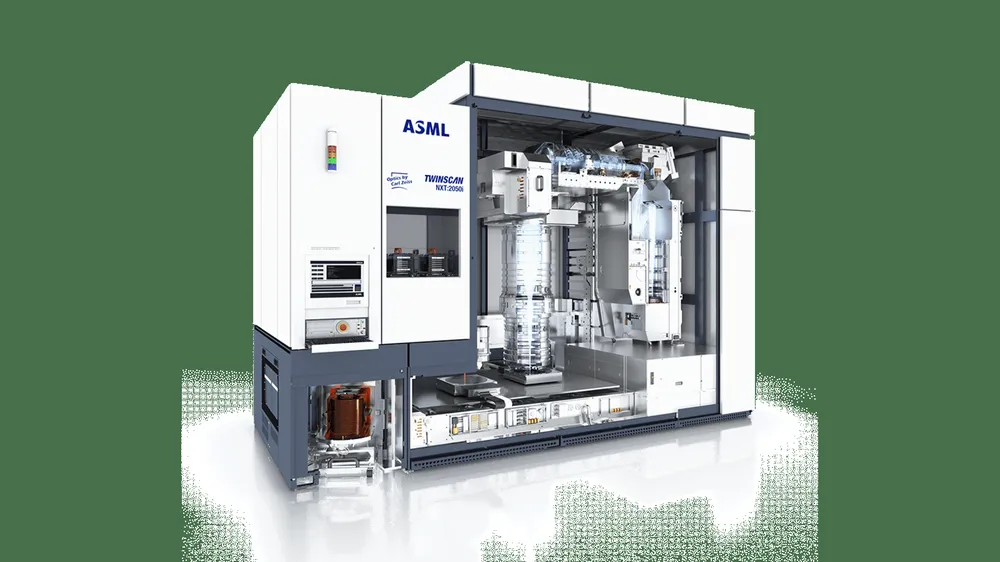
ASML NXT:2050i
ASML NXT:2050i: A Deep Dive into the State-of-the-Art Immersion Lithography System for 2024 Semiconductor Manufacturing
Executive Summary
The ASML NXT:2050i is a high-productivity, dual-stage immersion lithography tool designed for volume production of 300 mm wafers at advanced nodes. It features a numerical aperture (NA) of 1.35, the highest in the semiconductor industry, and is built on the future-proof NXT4 platform. The system combines high productivity with unprecedented overlay performance, making it a cost-effective solution for the manufacturing of 300 mm wafers at advanced Logic and DRAM nodes.
The NXT:2050i is capable of producing 295 wafers per hour, with the ability to deliver 400 to 500 additional wafers per day by reducing overhead times compared to earlier TWINSCAN systems. The system features a new immersion hood that reduces water loss, significantly improving defectivity performance and translating to improved product yield and higher productivity through fewer slowdowns.
Architecture & Design
The ASML NXT:2050i features a 1.35 NA 193 nm catadioptric projection lens that can achieve production resolutions down to 40 nm (C-quad) and 38 nm (dipole). The lens elements are equipped with manipulators to correct for optical aberrations, enabling maximum productivity for low-k1 imaging. The lens fingerprint is now optimized in high-density and can be matched towards EUV.
- The system features a dual-stage design, allowing for high-productivity and high-accuracy overlay performance.
- The Parallel ILIAS (PARIS) sensor allows for a parallel measurement of optical aberrations throughout the projection slit, enabling a more accurate alignment, enhanced reticle heating correction, and on-the-fly lens heating correction.
- The reticle stage is equipped with enhanced clamps, improving not only the reliability of the system but also the overlay.
- The ORION alignment sensor offers increased accuracy of alignment measurements and enhanced process robustness.
The NXT:2050i is built on the NXT4 platform, which provides a future-proof foundation for the system. The platform is designed to support the evolving needs of the semiconductor industry, with a focus on high-productivity, high-accuracy, and low-defectivity performance.
Performance & Thermal
The ASML NXT:2050i is capable of producing 295 wafers per hour, with the ability to deliver 400 to 500 additional wafers per day by reducing overhead times compared to earlier TWINSCAN systems. The system features a new immersion hood that reduces water loss, significantly improving defectivity performance and translating to improved product yield and higher productivity through fewer slowdowns.
- The system achieves production resolutions down to 40 nm (C-quad) and 38 nm (dipole).
- The lens elements are equipped with manipulators to correct for optical aberrations, enabling maximum productivity for low-k1 imaging.
- The system features a thermal management system, designed to maintain a stable temperature and minimize thermal drift.
- The system is equipped with a telemetry system, providing real-time monitoring and control of the system's performance and thermal parameters.
Specification not publicly disclosed: Exact thermal design power (TDP) of the system. Exact figures were not confirmed: Thermal limits of the system.
Market Positioning
The ASML NXT:2050i is positioned as a high-end immersion lithography tool, designed for volume production of 300 mm wafers at advanced nodes. The system is targeted at leading-edge semiconductor manufacturers, who require high-productivity, high-accuracy, and low-defectivity performance.
Direct competitors of the ASML NXT:2050i include other high-end immersion lithography tools, such as the Nikon NSR-S631E and the Canon FPA-6300ES6a. The exact target buyer of the system is not publicly disclosed, but it is likely to be leading-edge semiconductor manufacturers, such as Intel, Samsung, and TSMC.
Specifications
Technical Specifications
| Specification | Detail |
|---|---|
| Numerical Aperture (NA) | 1.35 |
| Wavelength | 193 nm |
| Resolution | Down to 40 nm (C-quad) and 38 nm (dipole) |
| Wafer Size | 300 mm |
| Throughput | 295 wafers per hour |
| Platform | NXT4 |
Frequently Asked Questions
Frequently Asked Questions
What is the numerical aperture (NA) of the ASML NXT:2050i?
The numerical aperture (NA) of the ASML NXT:2050i is 1.35, the highest in the semiconductor industry.
What is the resolution of the ASML NXT:2050i?
The ASML NXT:2050i can achieve production resolutions down to 40 nm (C-quad) and 38 nm (dipole).
What is the throughput of the ASML NXT:2050i?
The ASML NXT:2050i is capable of producing 295 wafers per hour, with the ability to deliver 400 to 500 additional wafers per day by reducing overhead times compared to earlier TWINSCAN systems.