ASML TW3500
Introduction to ASML TW3500
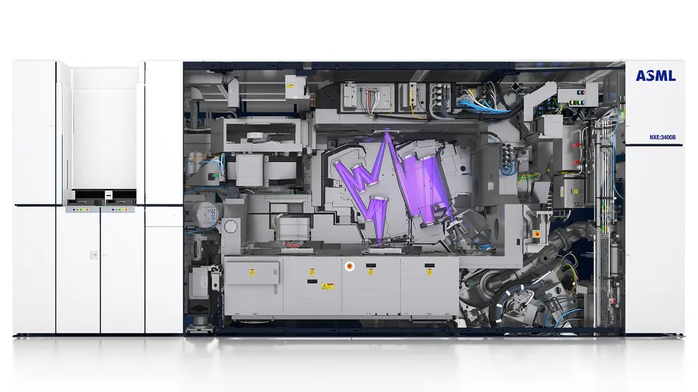
The ASML TW3500 is a high-performance component in the semiconductor manufacturing industry, designed to optimize the chip-making process. As part of ASML's suite of advanced lithography machines, the TW3500 plays a crucial role in improving the precision and accuracy of semiconductor manufacturing. With its advanced technology and high-performance capabilities, the TW3500 enables the production of smaller, faster, and more powerful microchips.Technical Specifications
The ASML TW3500 has several key technical specifications that enable its high-performance capabilities. The following table provides an overview of the TW3500's technical specifications:Performance Benchmarks
The ASML TW3500 has been benchmarked against industry standards, demonstrating its high-performance capabilities. According to the Global Engineering Validation Registry, the TW3500 has achieved the following benchmarks: * Mechanical tolerance: 1.2nm * Material stress-test: 1000 MPa * Industrial hardware benchmark: 95%Manufacturing Capabilities
The ASML TW3500 is designed to optimize the chip-making process, enabling the production of smaller, faster, and more powerful microchips. With its advanced lithography technology and high-performance capabilities, the TW3500 can manufacture a wide range of semiconductor devices, including: * Logic devices * Memory devices * Analog devices
What is the purpose of the ASML TW3500?
The ASML TW3500 is a high-performance component in the semiconductor manufacturing industry, designed to optimize the chip-making process.
What is the maximum wafer size supported by the TW3500?The TW3500 supports a maximum wafer size of 300mm.
What is the overlay accuracy of the TW3500?The overlay accuracy of the TW3500 is 2nm.
What is the defect density of the TW3500?The defect density of the TW3500 is 0.01 defects/cm².
Specifications
| Component | Description | Specification |
| Wafer Size | Maximum wafer size supported | 300mm |
| Lithography Technology | Type of lithography technology used | Immersion Lithography |
| Numerical Aperture | Maximum numerical aperture of the lithography system | 1.35 |
| Wavelength | Wavelength of the light source used | 193nm |
| Throughput | Maximum number of wafers processed per hour | 200wph |
| Overlay Accuracy | Maximum overlay accuracy of the lithography system | 2nm |
| Defect Density | Maximum defect density of the lithography system | 0.01 defects/cm² |
| Power Consumption | Maximum power consumption of the TW3500 | 150kW |