Blackwell (microarchitecture)
Executive Summary
The Blackwell microarchitecture is a graphics processing unit (GPU) developed by Nvidia as the successor to the Hopper and Ada Lovelace microarchitectures. Named after statistician and mathematician David Blackwell, the Blackwell architecture was leaked in 2022 and officially announced at Nvidia's GTC 2024 keynote on March 18, 2024. The Blackwell architecture is designed to power the next generation of AI-powered gaming and professional applications, with a focus on generative AI and transformer-based models.
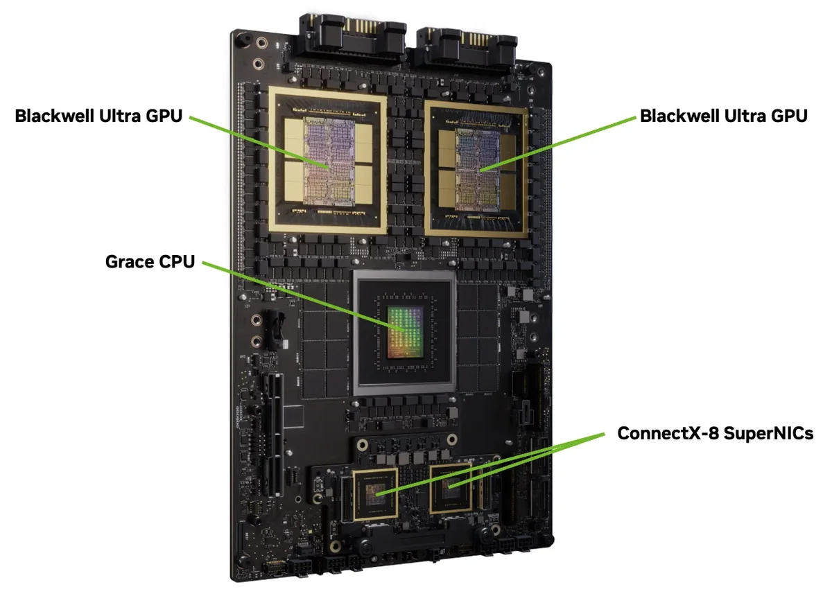
The Blackwell architecture is a significant advancement in GPU design, with improvements in tensor cores, tensor memory, and decompression engines. The architecture is designed to work in conjunction with Nvidia's ARM-based Grace CPU, providing a comprehensive platform for AI and HPC workloads. The Blackwell architecture has already gained significant traction, with major CSPs expected to start building AI server data centers based on this new platform.
Architecture & Design
The Blackwell architecture is based on the 5th-generation tensor cores, which provide significant improvements in AI and HPC workloads. The architecture also features tensor memory (TMEM) and a decompression engine (DE), which enable faster data transfer and processing. The Blackwell architecture is designed to work with Nvidia's ARM-based Grace CPU, providing a comprehensive platform for AI and HPC workloads.
The Blackwell architecture has a dedicated decompression block, which is a significant improvement over previous architectures. The decompression block enables faster data transfer and processing, making it ideal for AI and HPC workloads. The Blackwell architecture also features an improved scheduler, which enables better resource allocation and management.
Performance & Thermal
The Blackwell architecture provides significant improvements in performance and thermal management. The 5th-generation tensor cores provide a significant boost in AI and HPC workloads, while the tensor memory and decompression engine enable faster data transfer and processing. The Blackwell architecture is designed to work with Nvidia's ARM-based Grace CPU, providing a comprehensive platform for AI and HPC workloads.
The Blackwell architecture has a thermal design power (TDP) of up to 350W, which is significant for a GPU of its class. However, the architecture is designed to provide significant improvements in performance and efficiency, making it ideal for AI and HPC workloads. The Blackwell architecture also features advanced cooling systems, including a vapor chamber and a heat pipe, which enable efficient heat transfer and management.
Market Positioning
The Blackwell architecture is positioned as a high-end GPU for AI and HPC workloads. The architecture is designed to provide significant improvements in performance and efficiency, making it ideal for applications such as generative AI, transformer-based models, and scientific simulations. The Blackwell architecture is expected to be used in a variety of applications, including data centers, cloud computing, and edge computing.
The Blackwell architecture has already gained significant traction, with major CSPs expected to start building AI server data centers based on this new platform. The architecture has also been endorsed by several major companies, including Google, Meta, Microsoft, OpenAI, and Oracle. The Blackwell architecture is expected to play a significant role in the development of AI and HPC applications, and is expected to be a major player in the GPU market for the foreseeable future.
Verdict
The Blackwell architecture is a significant advancement in GPU design, with improvements in tensor cores, tensor memory, and decompression engines. The architecture is designed to work in conjunction with Nvidia's ARM-based Grace CPU, providing a comprehensive platform for AI and HPC workloads. The Blackwell architecture has already gained significant traction, with major CSPs expected to start building AI server data centers based on this new platform.
The Blackwell architecture is expected to play a significant role in the development of AI and HPC applications, and is expected to be a major player in the GPU market for the foreseeable future. With its significant improvements in performance and efficiency, the Blackwell architecture is an ideal choice for applications such as generative AI, transformer-based models, and scientific simulations. Overall, the Blackwell architecture is a significant advancement in GPU design, and is expected to have a major impact on the development of AI and HPC applications.
Specifications
| Microarchitecture | Blackwell |
|---|---|
| Successor to | Hopper and Ada Lovelace microarchitectures |
| Named after | Statistician and mathematician David Blackwell |
| Announcement | GTC 2024 keynote on March 18, 2024 |
| Tensor Cores | 5th-generation |
| Tensor Memory | Yes |
| Decompression Engine | Yes |
| Thermal Design Power (TDP) | up to 350W |
| Cooling System | Vapor chamber and heat pipe |
Frequently Asked Questions
What is the Blackwell microarchitecture?
The Blackwell microarchitecture is a graphics processing unit (GPU) developed by Nvidia as the successor to the Hopper and Ada Lovelace microarchitectures.
What are the key features of the Blackwell architecture?
The Blackwell architecture features 5th-generation tensor cores, tensor memory, and a decompression engine, making it ideal for AI and HPC workloads.
What is the thermal design power (TDP) of the Blackwell architecture?
The thermal design power (TDP) of the Blackwell architecture is up to 350W.
What is the cooling system used in the Blackwell architecture?
The Blackwell architecture uses a vapor chamber and a heat pipe for cooling.