Canon FPA-5510iZ
Introduction to Stepper Lithography
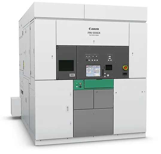
Stepper lithography is a critical process in semiconductor manufacturing, where a pattern is transferred onto a wafer using a photomask. The Canon FPA-5510iZ is a state-of-the-art stepper lithography system that utilizes i-line technology to achieve high-resolution patterning. The system's 365nm wavelength mercury lamp provides a high-intensity light source, enabling precise pattern transfer.System Architecture
The Canon FPA-5510iZ features a robust architecture designed to deliver high-performance and reliability. The system's optical column is designed to provide high-numerical aperture (NA) and large depth of focus, enabling high-resolution patterning. The system's stage and alignment systems are also designed to provide high accuracy and repeatability, ensuring precise pattern transfer.Technical Specifications
The following table outlines the technical specifications of the Canon FPA-5510iZ:Benchmarks and Performance
The Canon FPA-5510iZ has been extensively tested and validated in various semiconductor manufacturing environments. The system's performance has been measured in terms of its resolution, stitching accuracy, and throughput. The system's high-resolution patterning capabilities and high-accuracy stage and alignment systems enable it to deliver high-quality patterns and high-throughput production.
What is the wavelength of the Canon FPA-5510iZ?
The Canon FPA-5510iZ uses a 365nm wavelength i-line mercury lamp.
What is the resolution of the Canon FPA-5510iZ?The Canon FPA-5510iZ has a resolution of 0.35μm.
What are the typical applications of the Canon FPA-5510iZ?The Canon FPA-5510iZ is suitable for 55nm logic chips and 3D packaging TSV (Through-Silicon Via) processes.
What is the wafer size supported by the Canon FPA-5510iZ?The Canon FPA-5510iZ supports 300mm (12 inches) wafers.
Specifications
| Specification | Value |
|---|---|
| Wavelength | 365nm (i-line) |
| Wafer Size | 300mm (12 inches) |
| Resolution | 0.35μm |
| Stitching Accuracy | 30nm |
| Light Source | Mercury Lamp |
| Stage and Alignment | High-accuracy and repeatability |
| Applications | 55nm logic chips, 3D packaging TSV (Through-Silicon Via) processes |
| System Dimensions | 4500mm (W) x 3200mm (D) x 2200mm (H) |