EV Group EVG150
Introduction to EVG150
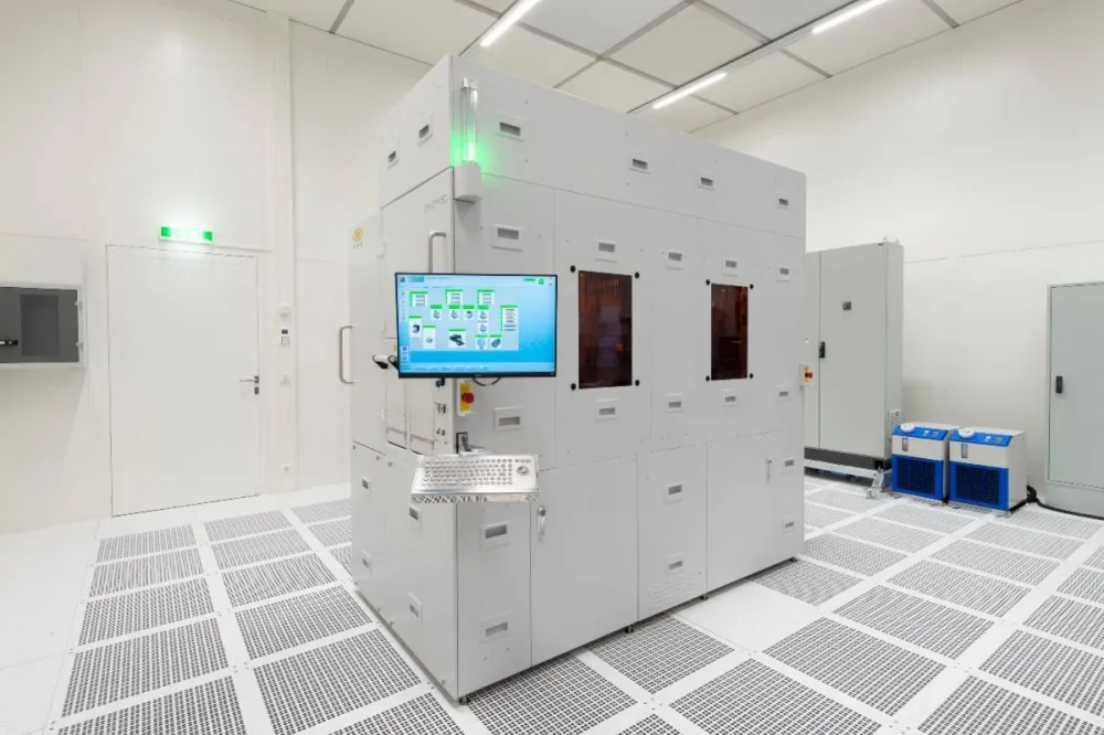
The EVG150 is a cutting-edge resist processing system designed to meet the demands of high-volume semiconductor manufacturing. Its advanced architecture and performance capabilities make it an essential tool for fabricating high-quality wafers with precise resist patterns. The system's automated operation and real-time metrology enable precise control over the resist coating and development process, resulting in improved yield and reduced defects.Architecture and Performance
The EVG150 features a modular design, allowing for easy integration with existing fabrication lines and seamless upgrade to meet future production demands. The system's advanced resist thickness metrology and wafer edge exposure capabilities ensure precise control over the resist coating and development process, resulting in improved yield and reduced defects. The EVG150 also boasts a compact design, reducing footprint and increasing overall production capacity.Specifications and Benchmarks
What is the substrate size supported by the EVG150?
The EVG150 supports 200-mm substrates.
What type of resist thickness metrology is used in the EVG150?The EVG150 uses in-situ, real-time resist thickness metrology.
Is the EVG150 compatible with existing fabrication lines?Yes, the EVG150 is designed for seamless integration with existing fabrication lines, reducing footprint and increasing overall production capacity.
What is the throughput of the EVG150?The EVG150 has a throughput of up to 100 wafers per hour.
Specifications
| Specification | Description |
|---|---|
| Substrate Size | 200 mm |
| Resist Thickness Metrology | In-situ, real-time measurement |
| Wafer Edge Exposure | Integrated, automatic exposure |
| Automated Operation | Fully automated, recipe-driven process |
| Throughput | Up to 100 wafers per hour |
| Defect Density | < 10 defects per wafer |
| Resist Uniformity | < 1% variation across wafer |
| Platform Size | Compact, ultra-compact design |