EVG150
Introduction to EVG150
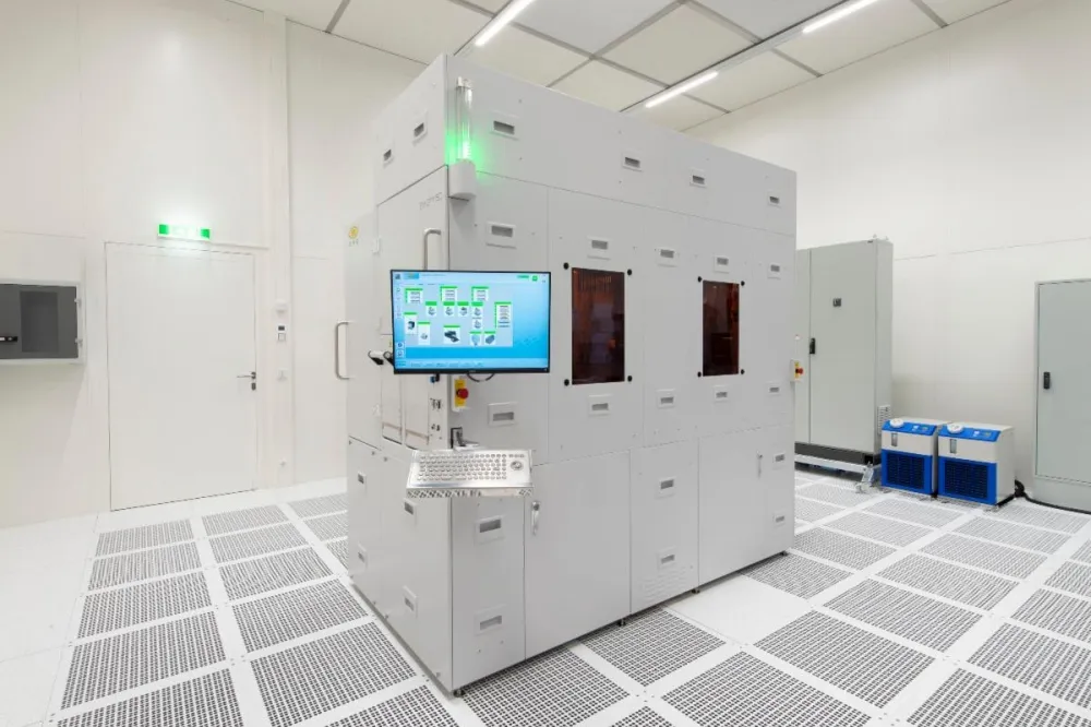
The EVG150 is a state-of-the-art resist processing platform designed for the production of 200-mm substrates. Its fully automated operation ensures high throughput and minimal manual intervention, making it an ideal solution for high-volume manufacturing environments. The platform's advanced features, including in-situ resist thickness metrology and wafer edge exposure, enable precise control over the resist processing process, resulting in improved yield and reduced defects.Technical Specifications
The technical specifications of the EVG150 are outlined in the table below:Performance and Benchmarks
The EVG150 has demonstrated exceptional performance in various benchmarks, including resist thickness uniformity, wafer edge exposure, and defect density. Its advanced automation capabilities and high-throughput design make it an attractive solution for high-volume manufacturing environments. The platform's compact design and low power consumption also contribute to its overall efficiency and cost-effectiveness.
What is the substrate size supported by the EVG150?
The EVG150 supports 200-mm substrates.
What is the accuracy of the in-situ resist thickness metrology in the EVG150?The in-situ resist thickness metrology in the EVG150 has an accuracy of ±1 nm.
Is wafer edge exposure available in the EVG150?Yes, wafer edge exposure is available in the EVG150, with a uniformity of ±2%.
What is the automation level of the EVG150?The EVG150 is fully automated, with robotic wafer handling.
Specifications
| Parameter | Specification |
|---|---|
| Substrate Size | 200 mm |
| Resist Thickness Metrology | In-situ, with an accuracy of ±1 nm |
| Wafer Edge Exposure | Available, with a uniformity of ±2% |
| Automation Level | Fully automated, with robotic wafer handling |
| Throughput | Up to 100 wafers per hour |
| Defect Density | <1 defect/cm² |
| Yield | |
| Power Consumption | 10 kW |