EVG40NT
Introduction to EVG40NT
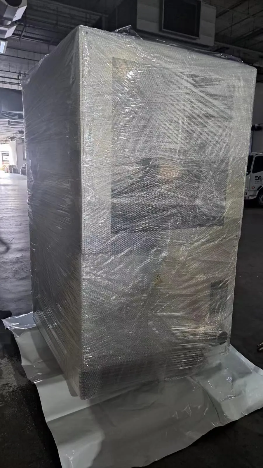
The EVG40NT is a semi-automated measurement system designed to provide high-accuracy measurements for various semiconductor manufacturing processes. This system is part of the EVG family of products, which are renowned for their high performance and reliability. The EVG40NT is equipped with advanced features that enable it to handle complex measurement tasks with ease, making it an ideal choice for manufacturers seeking to improve their production efficiency.Key Features and Specifications
The EVG40NT boasts an impressive array of features, including high measurement accuracy, diverse measurement methods, and adaptability to various manufacturing processes. Some of its key specifications include:Applications and Benefits
The EVG40NT is designed to cater to the needs of the semiconductor industry, providing high-accuracy measurements for various manufacturing processes. Its applications include: * Nanoimprint lithography * Wafer-to-wafer bonding * Semiconductor device manufacturing * Packaging and assembly The benefits of using the EVG40NT include: * Improved production efficiency * Enhanced product quality * Reduced costs * Increased yield
What is the measurement accuracy of the EVG40NT?
The EVG40NT offers high measurement accuracy, enabling verification of compliance to tight process specifications.
What types of measurement methods are supported by the EVG40NT?The EVG40NT supports a diverse range of measurement methods, including nanoimprint lithography and wafer-to-wafer bonding.
Can the EVG40NT be used for various manufacturing processes?Yes, the EVG40NT is adaptable to various manufacturing processes, including semiconductor device manufacturing and packaging.
How does the EVG40NT contribute to improved production efficiency?The EVG40NT enables high-efficiency measurements, allowing manufacturers to optimize their production processes and improve overall yield.
Specifications
| Parameter | Value |
|---|---|
| Measurement Accuracy | High accuracy, enabling verification of compliance to tight process specifications |
| Measurement Methods | Diverse range of methods, including nanoimprint lithography and wafer-to-wafer bonding |
| Manufacturing Processes | Adaptable to various processes, including semiconductor device manufacturing and packaging |
| System Configuration | Semi-automated, allowing for efficient and accurate measurements |
| Process Conditions | Able to handle various process conditions, including temperature, pressure, and humidity |
| Materials | Compatible with a wide range of materials, including silicon, glass, and other semiconductor materials |
| Efficiency | High efficiency, enabling improved production yield and reduced costs |
| Optimization | Enables optimization of integrated process parameters, ensuring high-quality semiconductor devices |