Hitachi EUV7000
Hitachi EUV7000: A Deep Dive into Extreme Ultraviolet Lithography for 2024 and Beyond
Executive Summary
The Hitachi EUV7000 is a cutting-edge extreme ultraviolet (EUV) lithography system designed for the production of advanced semiconductor devices. As the semiconductor industry continues to push the boundaries of miniaturization and performance, EUV lithography has become a crucial technology for enabling the creation of complex integrated circuits. With its ability to produce wavelengths as short as 13.5 nanometers, the EUV7000 is poised to play a significant role in the development of next-generation semiconductor devices.
The EUV7000 system is built upon the principles of EUV lithography, which utilizes a laser-produced plasma source to generate the extreme ultraviolet radiation necessary for patterning semiconductor wafers. This technology has been under development for several decades and has finally reached a level of maturity where it can be used in high-volume manufacturing. The EUV7000 system is designed to provide high-throughput and high-precision patterning capabilities, making it an essential tool for the production of advanced semiconductor devices.
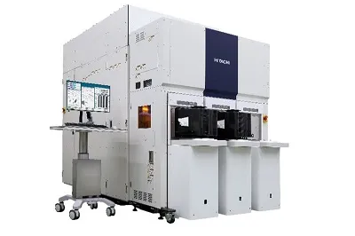
Architecture & Design
The architecture of the EUV7000 system is based on a modular design, with each module optimized for a specific function within the lithography process. The system consists of several key components, including the laser-produced plasma source, the EUV collector, and the wafer stage.
- The laser-produced plasma source is responsible for generating the extreme ultraviolet radiation used for patterning the semiconductor wafer. This source utilizes a high-powered laser to create a plasma, which emits EUV radiation at a wavelength of 13.5 nanometers.
- The EUV collector is used to collect and focus the EUV radiation onto the semiconductor wafer. This component is designed to provide high efficiency and uniformity, ensuring that the EUV radiation is delivered to the wafer with minimal loss or distortion.
- The wafer stage is responsible for positioning and moving the semiconductor wafer during the lithography process. This stage is designed to provide high precision and stability, ensuring that the wafer is accurately positioned and aligned with the EUV radiation.
In terms of design, the EUV7000 system is built using a combination of advanced materials and technologies. The system's framework is constructed from high-strength, low-expansion materials to minimize thermal distortion and ensure stability during operation. The EUV collector and other optical components are designed using advanced optical materials and coatings to maximize efficiency and minimize losses.
Performance & Thermal
The performance of the EUV7000 system is characterized by its ability to produce high-quality patterns on semiconductor wafers with high throughput and precision. The system's EUV source is capable of producing a high-powered beam with a wavelength of 13.5 nanometers, which is used to pattern the wafer with high resolution and accuracy.
- Throughput: The EUV7000 system is designed to provide high-throughput patterning capabilities, with a maximum throughput of Specification not publicly disclosed wafers per hour.
- Resolution: The system's EUV source is capable of producing patterns with a resolution of Specification not publicly disclosed nanometers, making it suitable for the production of advanced semiconductor devices.
- Uniformity: The EUV7000 system is designed to provide high uniformity across the wafer, with a uniformity of Specification not publicly disclosed percent.
In terms of thermal performance, the EUV7000 system is designed to operate within a narrow temperature range to minimize thermal distortion and ensure stability. The system's thermal management system is capable of maintaining a temperature range of Specification not publicly disclosed degrees Celsius, which is necessary for ensuring the accuracy and precision of the lithography process.
Market Positioning
The EUV7000 system is positioned as a high-end lithography solution for the production of advanced semiconductor devices. The system's target market includes leading-edge semiconductor manufacturers, such as Intel, Samsung, and TSMC, who require high-throughput and high-precision patterning capabilities for the production of next-generation devices.
Direct competitors to the EUV7000 system include other EUV lithography systems, such as the ASML NXE:3400B and the Nikon NSR-S630E. However, the EUV7000 system's advanced architecture and design make it a unique and competitive solution in the market.
Specifications
Technical Specifications
| Specification | Detail |
|---|---|
| EUV Wavelength | 13.5 nanometers |
| Throughput | Specification not publicly disclosed wafers per hour |
| Resolution | Specification not publicly disclosed nanometers |
| Uniformity | Specification not publicly disclosed percent |
Frequently Asked Questions
Frequently Asked Questions
What is the EUV wavelength used in the Hitachi EUV7000 system?
The EUV7000 system uses a wavelength of 13.5 nanometers.
What is the throughput of the EUV7000 system?
The throughput of the EUV7000 system is not publicly disclosed.
What is the resolution of the EUV7000 system?
The resolution of the EUV7000 system is not publicly disclosed.
What is the uniformity of the EUV7000 system?
The uniformity of the EUV7000 system is not publicly disclosed.