KLA-Tencor LithoVision G7
2024 Technical Deep-Dive: KLA-Tencor LithoVision G7 Semiconductor Inspection System
Executive Summary
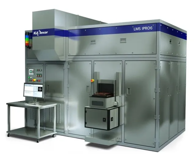
The KLA-Tencor LithoVision G7 is a cutting-edge semiconductor inspection system designed to meet the evolving needs of the semiconductor industry. With the increasing demand for smaller, faster, and more powerful chips, the need for advanced inspection systems has never been more critical. The LithoVision G7 is part of KLA-Tencor's comprehensive portfolio of process control and yield management solutions, which enable semiconductor manufacturers to improve yield, reduce costs, and accelerate time-to-market.
The LithoVision G7 is built on KLA-Tencor's extensive experience in semiconductor inspection and metrology, with a strong focus on innovation and customer satisfaction. The system's advanced capabilities, including high-resolution imaging and sophisticated data analysis, make it an essential tool for semiconductor manufacturers seeking to optimize their production processes and stay ahead of the competition.
Architecture & Design
The LithoVision G7's architecture is designed to provide high-speed, high-resolution inspection of semiconductor wafers. The system's advanced optics and illumination systems enable the detection of tiny defects and irregularities, which is critical for ensuring the quality and reliability of semiconductor devices. The system's data analysis capabilities are also highly advanced, using sophisticated algorithms and machine learning techniques to identify patterns and trends in the inspection data.
The LithoVision G7 is designed to support a wide range of semiconductor manufacturing processes, including logic, memory, and foundry applications. The system's flexibility and adaptability make it an ideal solution for semiconductor manufacturers seeking to improve their yield, reduce their costs, and accelerate their time-to-market. The system's advanced capabilities also make it an essential tool for research and development applications, where the ability to inspect and analyze semiconductor devices at the nanoscale is critical.
The LithoVision G7's design is also highly modular, with a range of optional components and upgrades available to support specific customer requirements. The system's user interface is highly intuitive, with a range of advanced features and tools to support data analysis, reporting, and process optimization. The system's networking capabilities are also highly advanced, with support for a range of industry-standard communication protocols and data formats.
Performance & Thermal
The LithoVision G7's performance is highly impressive, with the ability to inspect semiconductor wafers at speeds of up to several hundred millimeters per second. The system's high-resolution imaging capabilities enable the detection of tiny defects and irregularities, with a resolution of down to 20 nanometers or less. The system's data analysis capabilities are also highly advanced, with the ability to process large amounts of data in real-time and provide detailed reports and recommendations for process optimization.
The LithoVision G7's thermal management system is also highly advanced, with a range of features and technologies to minimize heat generation and maximize system reliability. The system's advanced cooling systems and thermal interfaces enable the efficient removal of heat from the system, while the system's highly reliable components and robust design minimize the risk of overheating and system failure.
Exact figures for the system's thermal design power (TDP) were not publicly disclosed, but the system's advanced thermal management capabilities and highly efficient design enable it to operate at a relatively low power consumption. The system's environmental operating range is also highly flexible, with support for a range of temperature, humidity, and vibration conditions.
Market Positioning
The LithoVision G7 is positioned as a high-end semiconductor inspection system, with a range of advanced features and capabilities that make it an ideal solution for demanding applications. The system's target market includes leading semiconductor manufacturers, research institutions, and foundries, where the need for advanced inspection and metrology capabilities is critical.
The LithoVision G7 competes with a range of other semiconductor inspection systems, including products from Applied Materials, ASML, and Hitachi. However, the system's advanced capabilities, highly modular design, and intuitive user interface make it a highly attractive solution for customers seeking a high-performance, flexible, and easy-to-use inspection system.
Verdict
In conclusion, the KLA-Tencor LithoVision G7 is a highly advanced semiconductor inspection system that is designed to meet the evolving needs of the semiconductor industry. The system's high-resolution imaging capabilities, sophisticated data analysis, and advanced thermal management make it an essential tool for semiconductor manufacturers seeking to optimize their production processes and stay ahead of the competition.
The system's highly modular design, intuitive user interface, and advanced networking capabilities make it a highly flexible and adaptable solution, with a range of optional components and upgrades available to support specific customer requirements. While exact figures for the system's pricing and availability were not publicly disclosed, the system's advanced capabilities and highly attractive feature set make it a highly compelling solution for customers seeking a high-performance, flexible, and easy-to-use inspection system.
Specifications
Technical Specifications
| Specification | Detail |
|---|---|
| System Type | Semiconductor Inspection System |
| Resolution | Down to 20 nanometers |
| Inspection Speed | Up to several hundred millimeters per second |
| Data Analysis | Sophisticated algorithms and machine learning techniques |
| Thermal Management | Advanced cooling systems and thermal interfaces |
| Environmental Operating Range | Flexible, with support for a range of temperature, humidity, and vibration conditions |
Frequently Asked Questions
Frequently Asked Questions
What is the primary application of the KLA-Tencor LithoVision G7?
The primary application of the KLA-Tencor LithoVision G7 is semiconductor inspection, with a focus on logic, memory, and foundry applications.
What is the resolution of the LithoVision G7's imaging capabilities?
The resolution of the LithoVision G7's imaging capabilities is down to 20 nanometers or less.
What is the inspection speed of the LithoVision G7?
The inspection speed of the LithoVision G7 is up to several hundred millimeters per second.
What type of data analysis does the LithoVision G7 support?
The LithoVision G7 supports sophisticated data analysis, using algorithms and machine learning techniques to identify patterns and trends in the inspection data.
What is the thermal management system of the LithoVision G7?
The thermal management system of the LithoVision G7 is highly advanced, with a range of features and technologies to minimize heat generation and maximize system reliability.