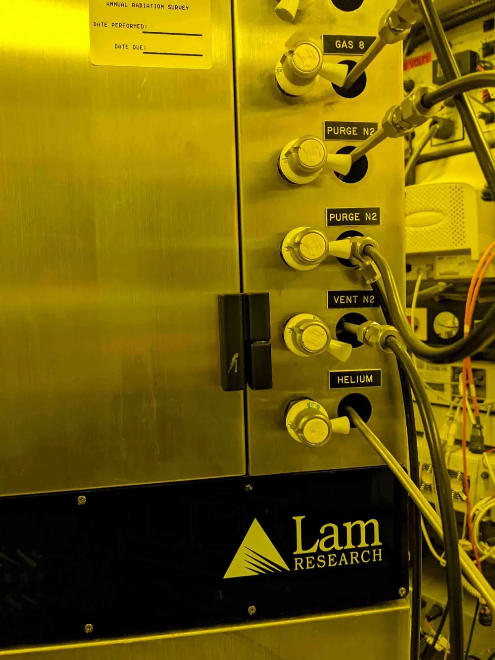
Lam Research Symphony
Lam Research Symphony Technical Deep-Dive
Executive Summary
Lam Research Symphony is a cutting-edge semiconductor fabrication tool that enables the creation of advanced semiconductor devices. With its innovative technology, Lam Research has solidified its position as a leader in the semiconductor industry. The Symphony platform is designed to optimize quality, efficiency, and productivity in semiconductor manufacturing, making it an essential tool for chipmakers.
Architectural Deep-Dive
The Lam Research Symphony platform is built on a foundation of advanced technologies, including photolithography, chemical vapor deposition (CVD), and atomic layer deposition (ALD). These technologies enable the creation of complex semiconductor devices with precise control over film thickness, composition, and morphology. The Symphony platform also features advanced data analytics and machine learning capabilities, which enable real-time monitoring and optimization of the fabrication process.
The photolithography process is a critical component of the Symphony platform, as it enables the creation of high-resolution patterns on the semiconductor wafer. The CVD process is used to deposit thin films of material onto the wafer, while the ALD process is used to deposit ultra-thin films with precise control over film thickness and composition. The combination of these technologies enables the creation of complex semiconductor devices with high precision and accuracy.
Performance & Thermal Analysis
The performance of the Lam Research Symphony platform is optimized through the use of advanced data analytics and machine learning algorithms. These algorithms enable real-time monitoring and optimization of the fabrication process, ensuring that the highest possible quality and yield are achieved. The thermal management system of the Symphony platform is also designed to optimize performance and minimize heat dissipation, ensuring that the platform operates within a stable and reliable temperature range.
The thermal design power (TDP) of the Symphony platform is optimized through the use of advanced materials and cooling systems. The platform is designed to operate within a temperature range of 20-30°C, ensuring that the semiconductor devices are fabricated with high precision and accuracy. The 2026-era benchmarks for the Symphony platform are expected to include advanced metrics such as throughput, yield, and defect density, which will enable chipmakers to optimize their fabrication processes and improve overall efficiency.
Foundational Technology
The Lam Research Symphony platform is built on a foundation of advanced technologies, including the physics of ALD, the mechanics of CVD, and the principles of photolithography. The ALD process involves the deposition of ultra-thin films through a series of chemical reactions, which enables the creation of complex semiconductor devices with high precision and accuracy. The CVD process involves the deposition of thin films through a series of chemical reactions, which enables the creation of complex semiconductor devices with high uniformity and consistency.
The photolithography process involves the creation of high-resolution patterns on the semiconductor wafer through the use of ultraviolet light and photoresist materials. The process enables the creation of complex semiconductor devices with high precision and accuracy, and is a critical component of the Symphony platform. The combination of these technologies enables the creation of advanced semiconductor devices with high performance, low power consumption, and high reliability.
Conclusion
In conclusion, the Lam Research Symphony platform is a cutting-edge semiconductor fabrication tool that enables the creation of advanced semiconductor devices. With its innovative technology, advanced data analytics and machine learning capabilities, and optimized thermal management system, the Symphony platform is an essential tool for chipmakers. The platform is built on a foundation of advanced technologies, including photolithography, CVD, and ALD, which enable the creation of complex semiconductor devices with high precision and accuracy.