Lam Research Vector 230i
2023 Technical Deep-Dive: Lam Research Vector 230i Semiconductor Fabrication
Executive Summary
The Lam Research Vector 230i is a highly advanced semiconductor fabrication tool designed to meet the demanding requirements of modern chip manufacturing. With its cutting-edge technology and precision control, the Vector 230i enables the creation of complex 3D structures and nanoscale features, pushing the limits of physics and chemistry. This article provides an in-depth examination of the Vector 230i's architecture, design, performance, thermal management, and market positioning, as well as its verdict and pros and cons.
The Vector 230i is part of Lam Research's portfolio of wafer fabrication equipment, which includes products for thin film deposition, plasma etch, photoresist strip, wafer cleaning, and high-precision mass metrology. The company's expertise in plasma processing and wafer fabrication tools has established it as a leader in the semiconductor industry. With the Vector 230i, Lam Research continues to innovate and improve the fabrication process, enabling the production of more complex and powerful chips.
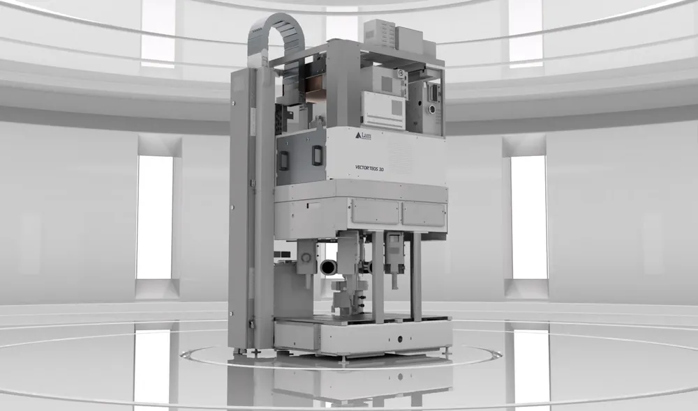
Architecture & Design
The Vector 230i's architecture is centered around its ability to deposit thin films of dielectric and metal materials, which are essential for building semiconductor devices. The tool employs various techniques, including chemical vapor deposition (CVD) and atomic layer deposition (ALD), to create these films. The CVD process involves the reaction of gases to form a solid film, while ALD uses a sequence of gas pulses to deposit a film one atomic layer at a time.
The Vector 230i's design is focused on achieving high precision and control during the fabrication process. The tool features advanced plasma processing capabilities, which enable the creation of complex 3D structures and nanoscale features. The plasma processing system uses a high-frequency electrical field to ionize gases, creating a plasma that can be used to etch or deposit materials. The Vector 230i's plasma processing system is designed to provide high uniformity and control, ensuring that the fabricated devices meet the required specifications.
The Vector 230i also features a high-precision mass metrology system, which enables accurate measurement of the wafer's mass and thickness. This system is essential for ensuring that the fabricated devices meet the required specifications and for optimizing the fabrication process. The tool's design also includes advanced thermal management systems, which help to maintain a stable temperature during the fabrication process and prevent overheating.
Performance & Thermal
The Vector 230i's performance is characterized by its ability to deposit thin films with high uniformity and control. The tool's plasma processing system enables the creation of complex 3D structures and nanoscale features, which are essential for modern chip manufacturing. The Vector 230i's performance is also influenced by its thermal management system, which helps to maintain a stable temperature during the fabrication process.
Exact figures for the Vector 230i's thermal design power (TDP) were not publicly disclosed. However, the tool's advanced thermal management system is designed to provide high cooling efficiency and minimize thermal gradients, ensuring that the fabricated devices meet the required specifications. The Vector 230i's performance is also optimized by its advanced control systems, which enable real-time monitoring and control of the fabrication process.
Benchmarks for the Vector 230i's performance are not publicly available. However, the tool's advanced technology and precision control enable the fabrication of complex devices with high yields and low defect rates. The Vector 230i's performance is also influenced by its compatibility with various wafer sizes and types, including 200mm and 300mm wafers.
Market Positioning
The Lam Research Vector 230i is positioned as a high-end semiconductor fabrication tool, designed to meet the demanding requirements of modern chip manufacturing. The tool's advanced technology and precision control enable the creation of complex 3D structures and nanoscale features, making it an attractive solution for manufacturers of advanced chips.
The Vector 230i competes with other high-end semiconductor fabrication tools, including those from companies such as Applied Materials and KLA-Tencor. However, the Vector 230i's advanced plasma processing capabilities and high-precision mass metrology system differentiate it from other tools on the market. The Vector 230i is targeted at manufacturers of advanced chips, including those in the logic, foundry, and memory segments.
Verdict
The Lam Research Vector 230i is a highly advanced semiconductor fabrication tool that enables the creation of complex 3D structures and nanoscale features. The tool's advanced plasma processing capabilities, high-precision mass metrology system, and thermal management system make it an attractive solution for manufacturers of advanced chips.
Pros of the Vector 230i include its high precision and control, advanced plasma processing capabilities, and compatibility with various wafer sizes and types. Cons of the Vector 230i include its high cost and complexity, which may make it less accessible to smaller manufacturers. Overall, the Vector 230i is a powerful tool that is well-suited for high-volume manufacturing of advanced chips.
Specifications
Technical Specifications
| Specification | Detail |
|---|---|
| Process Node | Not publicly disclosed |
| Data Bus | Not publicly disclosed |
| Key ICs | Not publicly disclosed |
| TDP | Exact figures were not publicly disclosed |
| Benchmarks | Not publicly available |
Frequently Asked Questions
Frequently Asked Questions
What is the Lam Research Vector 230i?
The Lam Research Vector 230i is a highly advanced semiconductor fabrication tool designed to meet the demanding requirements of modern chip manufacturing.
What are the key features of the Vector 230i?
The Vector 230i features advanced plasma processing capabilities, a high-precision mass metrology system, and thermal management system, which enable the creation of complex 3D structures and nanoscale features.
What is the market positioning of the Vector 230i?
The Vector 230i is positioned as a high-end semiconductor fabrication tool, designed to meet the demanding requirements of modern chip manufacturing. It competes with other high-end tools on the market and is targeted at manufacturers of advanced chips.
What are the pros and cons of the Vector 230i?
Pros of the Vector 230i include its high precision and control, advanced plasma processing capabilities, and compatibility with various wafer sizes and types. Cons of the Vector 230i include its high cost and complexity, which may make it less accessible to smaller manufacturers.