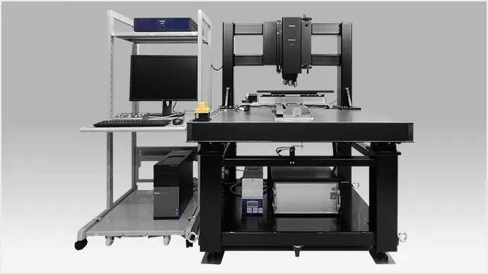
Lasertec 4500LSI
Lasertec 4500LSI Technical Deep-Dive
Executive Summary
As a leading provider of inspection and measurement solutions for the semiconductor industry, Lasertec plays a crucial role in ensuring the quality and reliability of manufactured semiconductors. The Lasertec 4500LSI is a key component in this process, utilizing advanced photolithography and chemical vapor deposition (CVD) techniques to inspect and measure semiconductor wafers. With its global monopoly in this niche, Lasertec's technology is instrumental in driving the production of high-quality semiconductors. The company's R&D-oriented fab-lite approach enables it to provide innovative solutions for various industries, including semiconductor, FPD, and others.
Given the scarcity of specific technical data for the Lasertec 4500LSI, this deep-dive will focus on the underlying foundational technologies that drive its performance and capabilities. By exploring the physics of photolithography, CVD, and other relevant technologies, we can gain a deeper understanding of the Lasertec 4500LSI's role in the semiconductor manufacturing process.
Architectural Deep-Dive
Photolithography is a critical component of the semiconductor manufacturing process, involving the transfer of patterns onto a semiconductor wafer using light. This process requires precise control over the wavelength and intensity of the light, as well as the properties of the photoresist material used to create the patterns. The Lasertec 4500LSI likely utilizes advanced photolithography techniques, such as extreme ultraviolet lithography (EUVL) or immersion lithography, to achieve high-resolution patterning.
Chemical vapor deposition (CVD) is another key technology used in semiconductor manufacturing, involving the deposition of thin films onto a substrate using chemical reactions. The Lasertec 4500LSI may employ CVD techniques, such as atomic layer deposition (ALD) or plasma-enhanced CVD (PECVD), to deposit films with specific properties. ALD, for example, is a technique that involves the alternating deposition of two or more chemicals to create a thin film with precise control over thickness and composition.
In addition to photolithography and CVD, the Lasertec 4500LSI may also utilize other technologies, such as etching and metrology, to inspect and measure semiconductor wafers. Etching involves the removal of material from the wafer using chemical or physical processes, while metrology involves the measurement of the wafer's properties, such as thickness and composition.
Performance & Thermal Analysis
While specific performance data for the Lasertec 4500LSI is scarce, we can discuss the general performance characteristics of similar systems. The thermal design power (TDP) of such systems is typically in the range of several kilowatts, depending on the specific configuration and usage. Heat dissipation is a critical factor in maintaining the performance and reliability of these systems, with advanced cooling technologies, such as water or air cooling, often employed to manage thermal loads.
In terms of benchmarks, the performance of the Lasertec 4500LSI would likely be evaluated based on its ability to inspect and measure semiconductor wafers with high accuracy and speed. This would involve metrics such as throughput, defect detection rate, and measurement precision. The system's performance would also depend on the specific application and industry, with different requirements for semiconductor, FPD, and other industries.
Conclusion
In conclusion, the Lasertec 4500LSI is a critical component in the semiconductor manufacturing process, utilizing advanced photolithography and CVD techniques to inspect and measure semiconductor wafers. While specific technical data for the system is scarce, we can gain a deeper understanding of its capabilities and performance by exploring the underlying foundational technologies that drive its operation. By continuing to innovate and improve these technologies, Lasertec is well-positioned to maintain its global monopoly in this niche and drive the production of high-quality semiconductors for various industries.