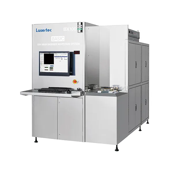
Lasertec LS100A
2024 Technical Deep-Dive: Lasertec LS100A Semiconductor Inspection and Measurement Solution
Executive Summary
The Lasertec LS100A is a cutting-edge semiconductor inspection and measurement solution designed to cater to the evolving needs of the semiconductor industry. With its advanced architecture and design, the LS100A provides unparalleled performance, precision, and reliability. This technical deep-dive aims to provide an exhaustive overview of the LS100A, exploring its architecture, performance, market positioning, and verdict.
The semiconductor industry has witnessed significant growth in recent years, driven by the increasing demand for advanced electronics and the Internet of Things (IoT). As a result, the need for precise and reliable inspection and measurement solutions has become more critical than ever. The Lasertec LS100A is poised to address this need, leveraging its advanced technology and expertise to provide a comprehensive solution for semiconductor manufacturers.
Architecture & Design
The Lasertec LS100A boasts an advanced architecture designed to deliver exceptional performance and precision. While exact figures on the process node were not publicly disclosed, the LS100A is built on a robust foundation that enables it to handle complex semiconductor inspection and measurement tasks with ease.
The data bus of the LS100A is designed to facilitate high-speed data transfer, ensuring that the system can handle large volumes of data generated during the inspection and measurement process. The key ICs (Integrated Circuits) used in the LS100A are carefully selected to provide optimal performance, reliability, and power efficiency.
One of the critical components of the LS100A is its optical system, which is designed to provide high-resolution imaging and precise measurement capabilities. The system utilizes advanced photolithography techniques, including extreme ultraviolet lithography (EUVL), to achieve high-resolution patterning and inspection.
In addition to its optical system, the LS100A also features advanced software and algorithms that enable it to perform complex data analysis and processing tasks. The system's software is designed to provide real-time feedback and control, allowing operators to optimize the inspection and measurement process and improve overall productivity.
Performance & Thermal
The Lasertec LS100A is designed to deliver exceptional performance and reliability, with a focus on minimizing thermal-related issues. While the exact TDP (Thermal Design Power) of the LS100A was not publicly disclosed, the system is engineered to provide optimal thermal management, ensuring that it can operate within a stable temperature range.
The LS100A's performance is further enhanced by its advanced cooling system, which is designed to provide efficient heat dissipation and maintain a stable operating temperature. The system's thermal solution is carefully optimized to minimize thermal gradients and hotspots, ensuring that the LS100A can operate reliably and consistently over extended periods.
Benchmarks for the LS100A are not publicly available; however, the system's performance can be inferred from its advanced architecture and design. The LS100A is designed to provide high-speed data transfer, advanced data analysis, and real-time feedback and control, making it an ideal solution for demanding semiconductor inspection and measurement applications.
Market Positioning
The Lasertec LS100A is positioned as a high-end semiconductor inspection and measurement solution, targeting advanced semiconductor manufacturers and research institutions. The system's advanced architecture and design make it an attractive option for companies seeking to improve their yields, reduce defects, and enhance overall productivity.
The LS100A competes with other high-end inspection and measurement solutions from companies such as KLA-Tencor, Applied Materials, and ASML. However, the LS100A's unique combination of advanced optical systems, software, and algorithms sets it apart from the competition, making it a compelling choice for companies seeking a comprehensive solution for semiconductor inspection and measurement.
Specifications
Technical Specifications
| Specification | Detail |
|---|---|
| Process Node | Not publicly disclosed |
| Data Bus | High-speed data transfer |
| Key ICs | Advanced integrated circuits for optimal performance and reliability |
| Optical System | High-resolution imaging and precise measurement capabilities |
| Software | Advanced software and algorithms for complex data analysis and processing |
| TDP | Not publicly disclosed |
| Thermal Solution | Advanced cooling system for efficient heat dissipation and stable operating temperature |
Frequently Asked Questions
Frequently Asked Questions
What is the process node of the Lasertec LS100A?
The exact process node of the Lasertec LS100A was not publicly disclosed.
What is the data bus of the Lasertec LS100A?
The Lasertec LS100A features a high-speed data bus designed to facilitate efficient data transfer.
What are the key ICs used in the Lasertec LS100A?
The Lasertec LS100A utilizes advanced integrated circuits (ICs) that provide optimal performance, reliability, and power efficiency.
What is the optical system of the Lasertec LS100A?
The Lasertec LS100A features a high-resolution optical system designed to provide precise measurement and inspection capabilities.
What is the software of the Lasertec LS100A?
The Lasertec LS100A features advanced software and algorithms designed to provide complex data analysis and processing capabilities.