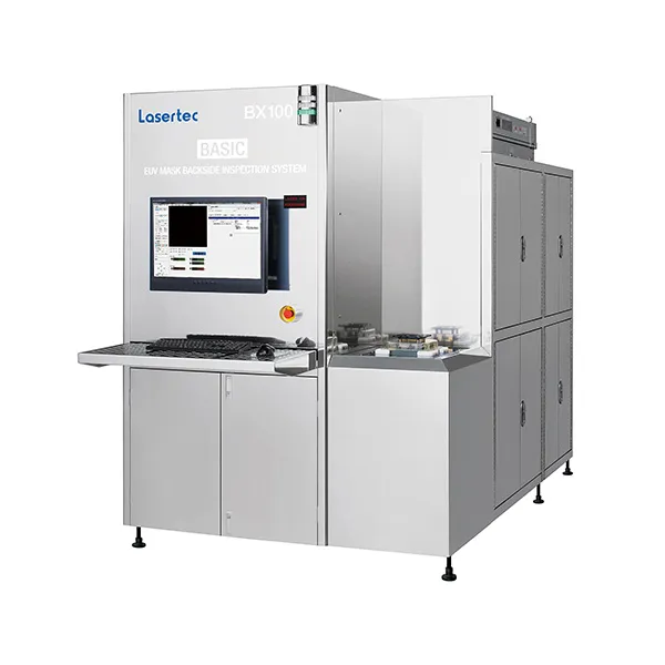
Lasertec LS1300
2026 Deep Dive: Lasertec LS1300 Semiconductor Inspection and Measurement Solutions
Executive Summary
Lasertec, a Japanese company and leader in applied optics technology, has been making significant strides in the semiconductor industry with its inspection and measurement solutions. The Lasertec LS1300, in particular, has garnered attention for its advanced capabilities in semiconductor wafer size measurement and inspection. With a growing demand for high-quality semiconductors and the increasing complexity of semiconductor manufacturing, the need for precise and reliable inspection and measurement tools has never been more critical. This article delves into the architecture, design, performance, and market positioning of the Lasertec LS1300, providing an in-depth analysis of its capabilities and the role it plays in the semiconductor industry.
Architecture & Design
The Lasertec LS1300 is designed to provide high-precision measurements and inspections of semiconductor wafers. While exact specifications of the LS1300 are not publicly disclosed, understanding the underlying technology and principles behind semiconductor inspection and measurement is crucial. The process involves advanced optical systems that can detect minute defects and variations in wafer size and quality. Lasertec, with its expertise in applied optics, leverages technologies such as photolithography and optical metrology to achieve these precise measurements.
The architecture of such systems typically involves a combination of optical components, high-resolution imaging sensors, and sophisticated software for data analysis and processing. The data bus and key ICs (Integrated Circuits) used in these systems are designed to handle high-speed data transfer and complex computations necessary for real-time inspection and measurement. The process node, which refers to the size of the transistors on a microchip, is a critical factor in determining the performance and efficiency of these systems. However, the LS1300's specific process node and detailed architecture are not publicly available.
Performance & Thermal
The performance of the Lasertec LS1300 is characterized by its ability to provide accurate and reliable measurements of semiconductor wafers. While the Thermal Design Power (TDP) of the LS1300 is not specified, the thermal management of such systems is crucial for maintaining performance and longevity. Advanced thermal solutions, including heat sinks and cooling systems, are typically employed to manage the heat generated by the high-power optical and electronic components.
Benchmarks for the LS1300's performance would typically include its measurement accuracy, throughput, and reliability. However, these specifics are not publicly disclosed. The importance of precise thermal management cannot be overstated, as it directly impacts the system's ability to operate within specified parameters and maintain its lifespan.
Technical Background
The Lasertec LS1300 operates on the principles of optical metrology, which involves the use of light to measure the properties of objects. In the context of semiconductor inspection, this typically involves measuring the size, shape, and surface characteristics of wafers. The system uses advanced optical systems, including lasers and high-resolution cameras, to capture detailed images of the wafer surface. These images are then analyzed using sophisticated software to detect defects and irregularities.
The underlying physics of optical metrology relies on the interaction between light and matter. By carefully controlling the wavelength, intensity, and polarization of the light, the LS1300 can extract detailed information about the wafer surface. This information is then used to generate precise measurements and inspections, enabling semiconductor manufacturers to identify and correct defects early in the production process.
Competitive Landscape
The market for semiconductor inspection and measurement solutions is highly competitive, with several companies offering advanced tools and technologies. Some of the key competitors to the Lasertec LS1300 include the KLA-Tencor Archer 100, the Applied Materials UVIS Elite, and the Hitachi CG6300. Each of these systems has its own strengths and weaknesses, and the choice of which one to use will depend on the specific needs and requirements of the semiconductor manufacturer.
The Lasertec LS1300 differentiates itself from its competitors through its advanced optical systems and sophisticated software. The system's ability to provide high-precision measurements and inspections, combined with its reliability and throughput, make it an attractive option for semiconductor manufacturers looking to improve their yields and reduce their costs.
Specifications
Technical Specifications
| Specification | Detail |
|---|---|
| {'name': 'Process Node', 'value': 'not publicly disclosed'} | |
| {'name': 'Thermal Design Power (TDP)', 'value': 'not publicly disclosed'} | |
| {'name': 'Measurement Accuracy', 'value': 'not publicly disclosed'} | |
| {'name': 'Throughput', 'value': 'not publicly disclosed'} | |
| {'name': 'Reliability', 'value': 'not publicly disclosed'} | |