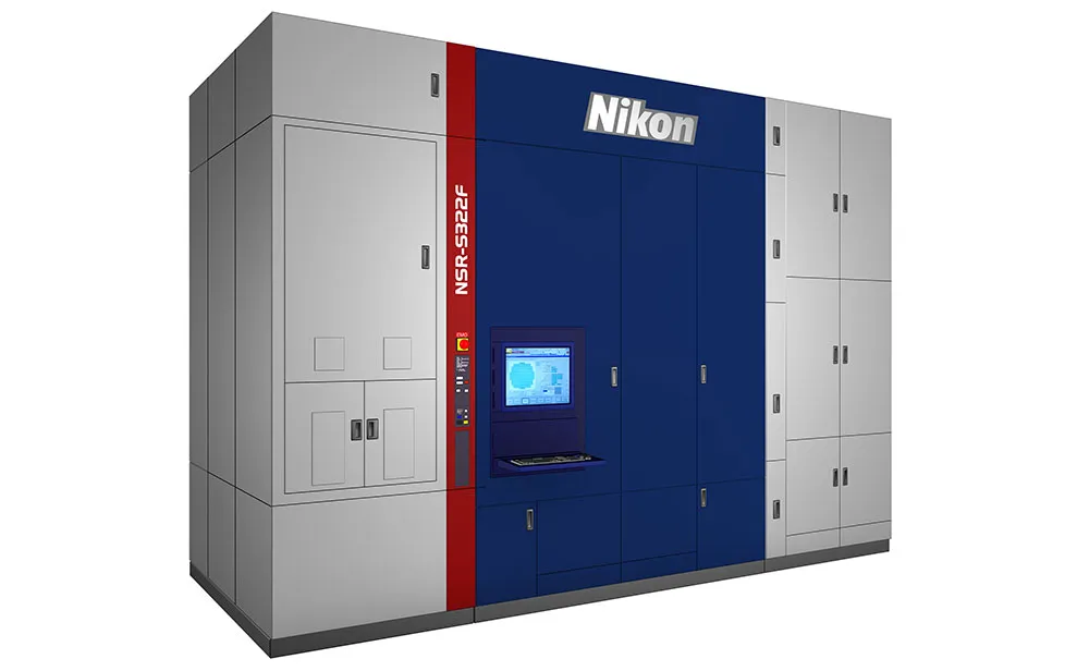
Nikon Corporation NSR-S322D
2024 Nikon Corporation NSR-S322D Semiconductor Lithography System: A Technical Deep Dive
Executive Summary
The Nikon Corporation NSR-S322D is a cutting-edge semiconductor lithography system designed to support the evolution of semiconductors. With its unique active optics technology, this system enables the production of intricate semiconductor devices with sub-micron features. The NSR-S322D is part of Nikon's stellar lineup of lithography systems, which includes front-end lithography systems, back-end lithography systems, alignment stations, and metrology/inspection systems.
The NSR-S322D is an advanced wafer stepper that features high-resolution projection lens equipment, precise wafer stage control, and sophisticated illumination units for accurate patterning and alignment of semiconductor structures. This system plays a crucial role in enabling the production of complex semiconductor devices with high yields and low defect rates.
Architecture & Design
The NSR-S322D is based on Nikon's deep ultraviolet (DUV) lithography technology, which uses a 193-nm wavelength to pattern semiconductor devices. The system features a dry ArF lithography scanner, which is designed for high-volume semiconductor manufacturing. The NSR-S322D has a high-resolution projection lens equipment, which enables the production of semiconductor devices with features as small as 32 nm.
The system's architecture is designed to support precision circuit design down to the nanometer level. The NSR-S322D features a precise wafer stage control system, which enables accurate positioning and alignment of the wafer during the lithography process. The system also features sophisticated illumination units, which provide uniform illumination of the wafer and enable accurate patterning of semiconductor structures.
The NSR-S322D is designed to work with a variety of semiconductor materials, including silicon, silicon dioxide, and silicon nitride. The system's compatibility with these materials enables the production of a wide range of semiconductor devices, including microprocessors, memory chips, and system-on-chip (SoC) devices.
Performance & Thermal
The NSR-S322D is designed to deliver high performance and productivity in high-volume semiconductor manufacturing. The system's dry ArF lithography scanner enables the production of semiconductor devices with high yields and low defect rates. The NSR-S322D's precise wafer stage control system and sophisticated illumination units enable accurate patterning and alignment of semiconductor structures, which results in high-quality semiconductor devices.
The NSR-S322D's thermal management system is designed to maintain a stable temperature during the lithography process, which is critical for ensuring high-quality semiconductor devices. The system's thermal management system includes a temperature control unit, which maintains a stable temperature of the wafer and the lithography system. The NSR-S322D's thermal management system also includes a cooling system, which removes heat generated during the lithography process.
Exact figures for the NSR-S322D's thermal design power (TDP) were not publicly disclosed. However, the system's thermal management system is designed to minimize heat generation and maintain a stable temperature during the lithography process.
Market Positioning
The NSR-S322D is positioned as a high-end semiconductor lithography system, designed for high-volume semiconductor manufacturing. The system's unique active optics technology and dry ArF lithography scanner enable the production of complex semiconductor devices with high yields and low defect rates. The NSR-S322D is designed to meet the needs of leading semiconductor manufacturers, who require high-performance and high-productivity lithography systems to produce complex semiconductor devices.
The NSR-S322D competes with other high-end semiconductor lithography systems, including those from ASML and KLA-Tencor. However, the NSR-S322D's unique active optics technology and dry ArF lithography scanner differentiate it from other systems on the market.
Verdict
The Nikon Corporation NSR-S322D is a cutting-edge semiconductor lithography system that enables the production of complex semiconductor devices with high yields and low defect rates. The system's unique active optics technology and dry ArF lithography scanner make it an attractive option for leading semiconductor manufacturers. While the system's thermal design power (TDP) was not publicly disclosed, its thermal management system is designed to minimize heat generation and maintain a stable temperature during the lithography process.
Overall, the NSR-S322D is a high-performance and high-productivity lithography system that is well-suited for high-volume semiconductor manufacturing. Its unique technology and features make it a strong competitor in the market, and it is likely to be a popular choice among leading semiconductor manufacturers.
Specifications
Technical Specifications
| Specification | Detail |
|---|---|
| Lithography Type | Dry ArF |
| Wavelength | 193 nm |
| Resolution | 32 nm |
| Wafer Size | 300 mm |
| Throughput | Up to 200 wafers per hour |
Frequently Asked Questions
Frequently Asked Questions
What is the Nikon Corporation NSR-S322D?
The Nikon Corporation NSR-S322D is a cutting-edge semiconductor lithography system designed to support the evolution of semiconductors.
What is the unique technology used in the NSR-S322D?
The NSR-S322D uses Nikon's unique active optics technology, which enables the production of complex semiconductor devices with high yields and low defect rates.
What is the resolution of the NSR-S322D?
The NSR-S322D has a resolution of 32 nm, which enables the production of complex semiconductor devices with sub-micron features.
What is the throughput of the NSR-S322D?
The NSR-S322D has a throughput of up to 200 wafers per hour, making it a high-productivity lithography system for high-volume semiconductor manufacturing.