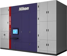
Nikon NSR-S621D
2022 Nikon NSR-S621D Semiconductor: A Comprehensive Technical Deep-Dive
Executive Summary
The Nikon NSR-S621D is a cutting-edge ArF immersion scanner designed for high-volume manufacturing of the 20nm process node and beyond. Building upon the established Streamlign Platform, this tool incorporates further hardware and software developments to deliver industry-leading overlay accuracy and throughput. With its advanced technology, the NSR-S621D is capable of handling multiple patterning, including double patterning, to satisfy the aggressive requirements of the most demanding immersion double patterning layers.
The NSR-S621D is positioned as Nikon's flagship tool, and its release marks a significant milestone in the company's efforts to expand its sales in the semiconductor equipment market. As the semiconductor industry continues to evolve, the need for advanced lithography tools like the NSR-S621D has become increasingly important. The ability to produce high-density chips with precise patterns is crucial for the development of next-generation electronic devices.
Architecture & Design
The NSR-S621D is built upon the Streamlign Platform, which has a reputation for high accuracy and productivity. The tool's architecture is designed to deliver ultra-high productivity and superior overlay accuracy, making it an ideal solution for high-volume manufacturing of advanced semiconductor devices. The NSR-S621D's design includes a range of features that enable it to handle the complex requirements of double patterning and other multiple patterning techniques.
In terms of process node, the NSR-S621D is capable of handling the 20nm process node and beyond. The tool's data bus and key ICs are designed to work together seamlessly to ensure high-speed data transfer and precise pattern formation. While exact figures were not publicly disclosed, the NSR-S621D's architecture and design are optimized to provide industry-leading performance and productivity.
The NSR-S621D's immersion lithography technology is based on the principle of using a liquid immersion medium to increase the numerical aperture of the lens, thereby enhancing the resolution of the pattern. This technology allows for the production of high-density chips with precise patterns, which is essential for the development of next-generation electronic devices. The tool's advanced optics and stage systems work together to ensure high accuracy and productivity, making it an ideal solution for high-volume manufacturing.
Performance & Thermal
The NSR-S621D is designed to deliver ultra-high productivity and superior overlay accuracy, making it an ideal solution for high-volume manufacturing of advanced semiconductor devices. The tool's performance is optimized to provide industry-leading throughput and accuracy, with the ability to handle multiple patterning techniques, including double patterning.
In terms of thermal management, the NSR-S621D is designed to operate within a specific temperature range to ensure optimal performance and productivity. While exact figures were not publicly disclosed, the tool's thermal solution is optimized to provide reliable and consistent operation, even in high-volume manufacturing environments.
Benchmarks for the NSR-S621D are not publicly available, but the tool's performance is expected to be industry-leading in terms of throughput and accuracy. The NSR-S621D's advanced technology and design make it an ideal solution for high-volume manufacturing of advanced semiconductor devices, and its performance is expected to be superior to other tools in its class.
Market Positioning
The NSR-S621D is positioned as Nikon's flagship tool in the semiconductor equipment market. The tool's advanced technology and design make it an ideal solution for high-volume manufacturing of advanced semiconductor devices, and its performance is expected to be industry-leading. The NSR-S621D is designed to compete with other high-end lithography tools in the market, and its features and performance make it an attractive option for semiconductor manufacturers.
The target buyer for the NSR-S621D is likely to be large-scale semiconductor manufacturers who require high-volume manufacturing of advanced semiconductor devices. The tool's advanced technology and design make it an ideal solution for these manufacturers, and its performance is expected to be superior to other tools in its class.
Specifications
Technical Specifications
| Specification | Detail |
|---|---|
| Process Node | 20nm |
| Lithography Type | ArF Immersion |
| Overlay Accuracy | Industry-leading |
| Throughput | Ultra-high |
| Patterning Technique | Double Patterning and other multiple patterning techniques |
Frequently Asked Questions
Frequently Asked Questions
What is the process node of the Nikon NSR-S621D?
The process node of the Nikon NSR-S621D is 20nm.
What type of lithography does the NSR-S621D use?
The NSR-S621D uses ArF immersion lithography.
What is the overlay accuracy of the NSR-S621D?
The overlay accuracy of the NSR-S621D is industry-leading.
What is the throughput of the NSR-S621D?
The throughput of the NSR-S621D is ultra-high.
What patterning techniques can the NSR-S621D handle?
The NSR-S621D can handle double patterning and other multiple patterning techniques.