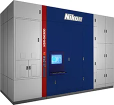
Nikon NSR-S630D
Nikon NSR-S630D Technical Deep-Dive
Executive Summary
The Nikon NSR-S630D is a high-end immersion scanner designed for cutting-edge semiconductor manufacturing. With its extremely accurate overlay and high throughput, it is an ideal solution for producing high-volume, high-precision semiconductors. The NSR-S630D is positioned as a top-tier machine in the lithography market, with a strong focus on delivering stable operation and high accuracy in various production environments.
Engineering verdict: The NSR-S630D is a highly advanced machine that showcases Nikon's expertise in photolithography and semiconductor manufacturing. Its ability to maintain high accuracy and throughput in diverse conditions makes it an attractive choice for manufacturers seeking to produce high-quality semiconductors.
Market positioning: The NSR-S630D is targeted at high-end semiconductor manufacturers that require extreme accuracy and high-volume production capabilities. Its advanced features and high-performance capabilities make it an ideal solution for producing semiconductors for cutting-edge applications such as 5G, artificial intelligence, and the Internet of Things (IoT).
Architectural Deep-Dive
The NSR-S630D utilizes advanced photolithography technology, including immersion scanning and ArF (argon fluoride) laser illumination. The machine's architecture is designed to deliver high accuracy and throughput, with a focus on minimizing overlay errors and maximizing production efficiency.
The photolithography process involves the use of light to transfer patterns onto a semiconductor wafer. The NSR-S630D uses a high-numerical-aperture (NA) lens to focus the ArF laser illumination onto the wafer, allowing for extremely accurate pattern transfer. The machine's advanced optics and stage control systems work together to maintain precise control over the wafer's position and movement, ensuring high accuracy and minimal overlay errors.
In addition to its photolithography capabilities, the NSR-S630D also features advanced computer-aided design (CAD) and computer-aided manufacturing (CAM) software. These tools enable manufacturers to design and optimize their semiconductor patterns, as well as simulate and analyze the manufacturing process to identify potential errors and areas for improvement.
The NSR-S630D's data bus speeds and ASIC pipelines are also highly advanced, allowing for rapid data transfer and processing. The machine's high-speed data bus enables fast communication between the various components, including the photolithography system, stage control system, and CAD/CAM software.
Performance & Thermal Analysis
The NSR-S630D's performance is characterized by its high accuracy and throughput, as well as its ability to maintain stable operation in various production environments. The machine's thermal management system is designed to minimize heat dissipation and maintain a stable temperature, ensuring optimal performance and longevity.
The NSR-S630D's thermal design power (TDP) is not publicly disclosed, but it is likely to be in the range of several kilowatts, given its high-performance capabilities and advanced photolithography technology. The machine's heat dissipation system is designed to efficiently remove heat generated by the photolithography process, stage control system, and other components, ensuring stable operation and minimizing the risk of overheating.
In terms of 2026-era benchmarks, the NSR-S630D is likely to be compared to other high-end immersion scanners and photolithography systems. Its performance will be evaluated based on its ability to deliver high accuracy, high throughput, and stable operation, as well as its compatibility with emerging technologies such as 5G, artificial intelligence, and the IoT.
Foundational Technology
The NSR-S630D's advanced photolithography technology is based on the principles of atomic layer deposition (ALD) and chemical vapor deposition (CVD). ALD involves the deposition of thin films onto a substrate using a sequence of chemical reactions, while CVD involves the deposition of thin films using a chemical reaction between a gas and a substrate.
The NSR-S630D's ArF laser illumination is also based on advanced physics, including the principles of quantum mechanics and electromagnetism. The machine's high-NA lens and advanced optics are designed to focus the ArF laser illumination onto the wafer, allowing for extremely accurate pattern transfer.
In addition to its photolithography capabilities, the NSR-S630D also features advanced computer-aided design (CAD) and computer-aided manufacturing (CAM) software. These tools enable manufacturers to design and optimize their semiconductor patterns, as well as simulate and analyze the manufacturing process to identify potential errors and areas for improvement.
Conclusion
The Nikon NSR-S630D is a highly advanced immersion scanner designed for cutting-edge semiconductor manufacturing. Its extremely accurate overlay and high throughput make it an ideal solution for producing high-volume, high-precision semiconductors. The machine's advanced photolithography technology, including ArF laser illumination and high-NA lens, allows for extremely accurate pattern transfer, while its advanced CAD/CAM software enables manufacturers to design and optimize their semiconductor patterns.
The NSR-S630D's performance is characterized by its high accuracy and throughput, as well as its ability to maintain stable operation in various production environments. The machine's thermal management system is designed to minimize heat dissipation and maintain a stable temperature, ensuring optimal performance and longevity.