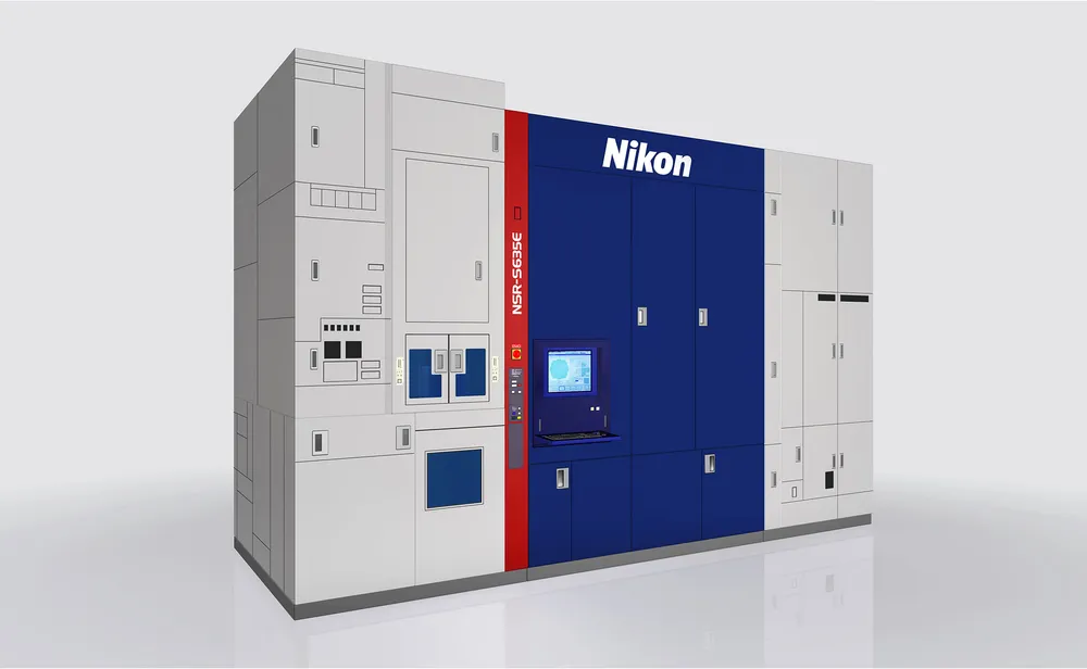
Nikon NSR-S635E
2023 Deep Dive: Nikon NSR-S635E Semiconductor Lithography System
Executive Summary
The Nikon NSR-S635E is a cutting-edge semiconductor lithography system released in 2018, designed to meet the ultra-high precision and productivity requirements of leading-edge semiconductor production. Leveraging the Streamlign Platform and advanced inline Alignment Station (iAS), this system delivers improved overlay accuracy and remarkable throughput. With its ability to handle 300mm wafers and support for ArF immersion lithography, the NSR-S635E is an essential tool for the production of advanced semiconductors.
The NSR-S635E is part of Nikon's lineup of lithography systems that support precision circuit design down to the nanometer level. Its development is a testament to Nikon's commitment to advancing semiconductor manufacturing technology. This system's capabilities make it an ideal choice for the production of a wide range of semiconductor devices, from NAND flash memory to advanced microprocessors.
Architecture & Design
The NSR-S635E's architecture is built around the Streamlign Platform, which provides a high-degree of flexibility and scalability. This platform enables the system to be easily integrated into existing production lines and facilitates the adoption of new technologies as they become available. The advanced inline Alignment Station (iAS) is a key component of the system, allowing for precise alignment of wafers and reticles to ensure optimal patterning performance.
The system's design also incorporates a hybrid measurement system, which combines the use of encoders and interferometers to achieve optimal stage performance. This approach enables the system to accurately measure the position of the reticle stage, reducing the effects of fluctuations in the air during each stage position measurement. Additionally, the use of 2D encoders for measuring the reticle stage position further enhances the system's accuracy and precision.
In terms of process node support, the NSR-S635E is capable of handling a wide range of nodes, from mature nodes like 28nm to more advanced nodes like 10nm and below. The system's support for ArF immersion lithography enables the production of devices with critical dimensions as small as 20nm. The NSR-S635E's data bus and key ICs are designed to provide high-speed data transfer and processing, ensuring that the system can handle the demands of high-volume production.
| Specification | Value |
|---|---|
| Process Node | 28nm and below |
| Lithography Type | ArF Immersion |
| Wafer Size | 300mm |
Performance & Thermal
The NSR-S635E's performance is characterized by its high throughput and precise patterning capabilities. The system is capable of achieving an overlay accuracy of less than 2.1nm, making it suitable for the production of advanced semiconductor devices. In terms of throughput, the NSR-S635E can process more than 275 wafers per hour (WPH), with 96 shots per wafer.
The system's thermal management is designed to minimize thermal effects and ensure stable operation. The exact thermal design power (TDP) of the NSR-S635E is not publicly disclosed, but it is designed to operate within a controlled temperature range to maintain optimal performance. The system's thermal solution is designed to provide efficient heat transfer and minimize thermal gradients, ensuring that the system can operate reliably over extended periods.
Benchmarks for the NSR-S635E are not publicly available, but the system's performance can be inferred from its specifications and capabilities. The system's ability to handle high-volume production and its support for advanced process nodes make it an ideal choice for the production of a wide range of semiconductor devices.
Market Positioning
The NSR-S635E is positioned as a high-end semiconductor lithography system, targeting leading-edge semiconductor manufacturers. The system's advanced capabilities and high precision make it an ideal choice for the production of advanced semiconductor devices, such as those used in artificial intelligence, 5G, and the Internet of Things (IoT).
The NSR-S635E competes with other high-end lithography systems from companies like ASML and Canon. However, Nikon's expertise in optics and its commitment to advancing semiconductor manufacturing technology make the NSR-S635E a unique and attractive option for manufacturers. The system's support for ArF immersion lithography and its ability to handle 300mm wafers make it an ideal choice for high-volume production.
Specifications
Technical Specifications
| Specification | Detail |
|---|---|
| Process Node | 28nm and below |
| Lithography Type | ArF Immersion |
| Wafer Size | 300mm |
| Overlay Accuracy | less than 2.1nm |
| Throughput | more than 275 WPH (96 shots) |
Frequently Asked Questions
Frequently Asked Questions
What is the Nikon NSR-S635E's process node support?
The NSR-S635E supports a wide range of process nodes, from mature nodes like 28nm to more advanced nodes like 10nm and below.
What type of lithography does the NSR-S635E support?
The NSR-S635E supports ArF immersion lithography, which enables the production of devices with critical dimensions as small as 20nm.
What is the NSR-S635E's wafer size support?
The NSR-S635E supports 300mm wafers, making it suitable for high-volume production.
What is the NSR-S635E's overlay accuracy?
The NSR-S635E's overlay accuracy is less than 2.1nm, making it suitable for the production of advanced semiconductor devices.
What is the NSR-S635E's throughput?
The NSR-S635E can process more than 275 wafers per hour (WPH), with 96 shots per wafer.