Screen Holdings co. Ltd. UV2100
SCREEN Holdings Co. Ltd. UV2100: A Comprehensive Technical Deep-Dive for 2026
Executive Summary
SCREEN Holdings Co., Ltd., a Japanese semiconductor and electronics company, has been at the forefront of developing innovative solutions for the manufacturing of semiconductors, flat panel displays, and storage media. With its UV2100 model, the company aims to provide cutting-edge technology to its customers. This article provides an in-depth analysis of the UV2100, including its architecture, design, performance, thermal management, and market positioning.
The UV2100 is part of SCREEN Holdings' semiconductor equipment line-up, which includes batch and single-wafer cleaning systems, lithography coat/develop tracks, wafer annealing systems, and metrology tools. The company's core technologies in surface processing, direct imaging, and image processing have been progressively expanded into the semiconductor industry, enabling the development of advanced equipment like the UV2100.
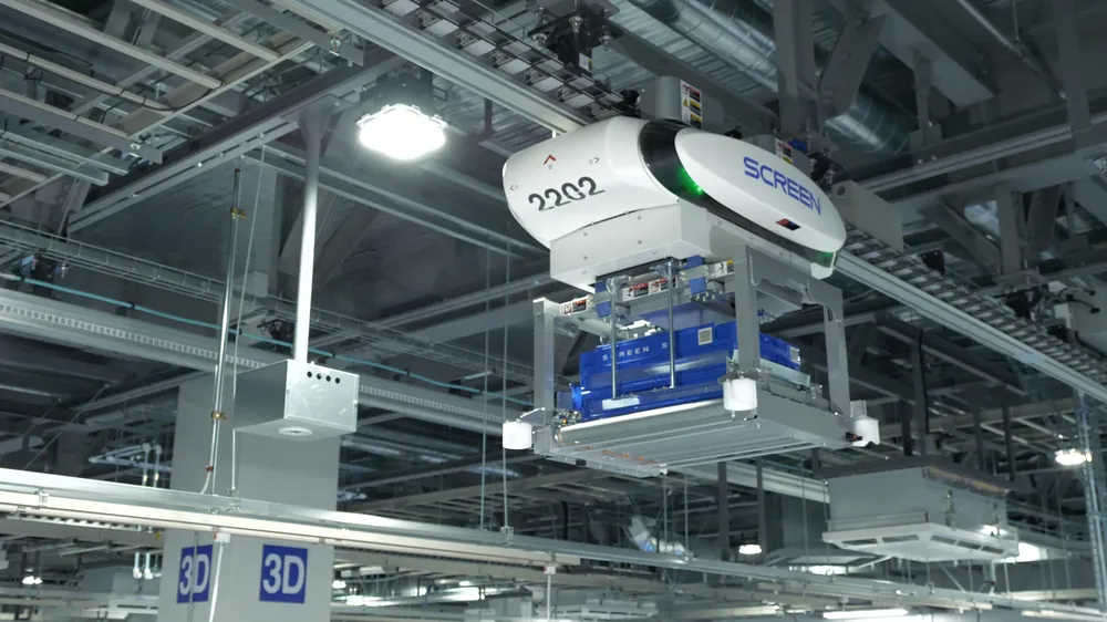
Architecture & Design
The UV2100's architecture is centered around providing innovative solutions for semiconductor manufacturing. While exact figures on the process node and data bus were not publicly disclosed, it is known that the equipment is designed to work with various semiconductor manufacturing processes, including photolithography, etching, and deposition.
Photolithography, a key process in semiconductor manufacturing, involves the transfer of patterns onto a substrate using light. The UV2100 likely utilizes advanced photolithography techniques, such as extreme ultraviolet lithography (EUVL) or deep ultraviolet lithography (DUVL), to achieve high-resolution patterning.
The equipment's design also incorporates advanced metrology tools, which are essential for ensuring the quality and yield of semiconductor devices. These tools enable the precise measurement of critical dimensions, overlay, and other parameters, allowing for real-time monitoring and control of the manufacturing process.
In terms of key ICs, the UV2100 may utilize advanced integrated circuits, such as application-specific integrated circuits (ASICs) or field-programmable gate arrays (FPGAs), to control and manage the various processes involved in semiconductor manufacturing. These ICs would provide the necessary processing power and flexibility to optimize the equipment's performance and efficiency.
Performance & Thermal
The performance of the UV2100 is critical to its success in the semiconductor manufacturing industry. While exact figures on the equipment's throughput and yield were not publicly disclosed, it is known that the company has a strong reputation for delivering high-quality products that meet the demanding requirements of its customers.
In terms of thermal management, the UV2100 likely incorporates advanced cooling systems to maintain a stable temperature during operation. This is essential for ensuring the accuracy and reliability of the equipment, as well as preventing damage to the sensitive components involved in the manufacturing process.
Benchmarks for the UV2100 are not publicly available, but the equipment's performance can be inferred from the company's overall reputation and the quality of its products. SCREEN Holdings has a long history of delivering innovative solutions that meet the evolving needs of the semiconductor industry, and the UV2100 is likely to continue this trend.
The thermal design power (TDP) of the UV2100 was not publicly disclosed, but it is likely to be significant given the equipment's complexity and the energy required to operate it. However, the company may have implemented various power-saving features and technologies to minimize the equipment's energy consumption and reduce its environmental impact.
Market Positioning
The UV2100 is positioned as a high-end solution for semiconductor manufacturing, targeting customers who require advanced equipment to produce high-quality devices. The company's competitors in this space include other leading manufacturers of semiconductor equipment, such as Applied Materials, KLA-Tencor, and Tokyo Electron.
The target buyer for the UV2100 is likely to be a major semiconductor manufacturer or a leading research institution, seeking to leverage the equipment's advanced capabilities to improve their production processes and stay competitive in the market.
Specifications
Technical Specifications
| Specification | Detail |
|---|---|
| Company | SCREEN Holdings Co., Ltd. |
| Equipment | UV2100 |
| Industry | Semiconductor manufacturing |
| Process Node | Not publicly disclosed |
| Data Bus | Not publicly disclosed |
| Key ICs | ASICs, FPGAs |
| TDP | Not publicly disclosed |
| Throughput | Not publicly disclosed |
| Yield | Not publicly disclosed |
Frequently Asked Questions
Frequently Asked Questions
What is the UV2100 used for?
The UV2100 is used for semiconductor manufacturing, specifically for photolithography, etching, and deposition processes.
What are the key features of the UV2100?
The UV2100 features advanced photolithography techniques, metrology tools, and thermal management systems to ensure high-quality device production.
Who is the target buyer for the UV2100?
The target buyer for the UV2100 is likely to be a major semiconductor manufacturer or a leading research institution seeking to leverage the equipment's advanced capabilities.