SCREEN Wafer Cleaning System SU-3200
Introduction to the SCREEN Wafer Cleaning System SU-3200
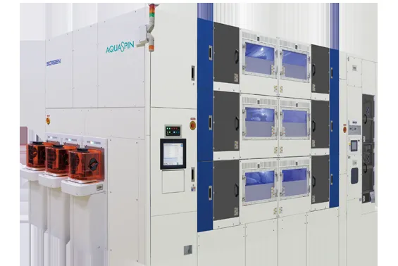
The SCREEN Wafer Cleaning System SU-3200 is a cutting-edge, hybrid-type cleaning system designed to meet the demanding requirements of advanced semiconductor manufacturing. The system combines chemical etching/cleaning functions with a brush cleaning function, providing a comprehensive cleaning solution for wafer backside cleaning and wet etch processes.Key Features and Specifications
The SCREEN Wafer Cleaning System SU-3200 boasts an impressive array of features and specifications, including:Performance and Benefits
The SCREEN Wafer Cleaning System SU-3200 offers a range of benefits, including high throughput, flexibility, and scalability. Its ability to support wafer backside cleaning and wet etch processes makes it an essential tool in the fabrication of advanced semiconductor devices. The system's high-performance capabilities and advanced features ensure defect-free surfaces after thin-film or dielectric layers are applied, supporting the production of next-generation memory, logic, and power devices.
What is the throughput of the SCREEN Wafer Cleaning System SU-3200?
The SCREEN Wafer Cleaning System SU-3200 has a throughput of up to 800 wafers per hour.
What types of cleaning functions does the SU-3200 support?The SU-3200 supports chemical etching/cleaning functions and brush cleaning functions.
What is the market projection for the semiconductor single wafer cleaner market?The semiconductor single wafer cleaner market is projected to grow at a CAGR of 6% from 2026 to 2033.
What is the application of the SCREEN Wafer Cleaning System SU-3200?The SCREEN Wafer Cleaning System SU-3200 is designed for advanced semiconductor manufacturing.
Specifications
| Feature | Specification |
|---|---|
| Throughput | Up to 800 wafers per hour |
| Expandability | Up to 12 chambers |
| Chemical Supply System | Dynamic direct injection (DDI) or cabinet-type |
| Wafer Size | 300mm |
| Cleaning Functions | Chemical etching/cleaning and brush cleaning |
| Processes Supported | Wafer backside cleaning and wet etch processes |
| Application | Advanced semiconductor manufacturing |
| Market Projection | Projected to grow at a CAGR of 6% from 2026 to 2033 |