TEL TRIAS SP
TEL TRIAS SP: A Comprehensive Technical Deep-Dive for 2026 Semiconductor Fabrication
Executive Summary
The TEL TRIAS SP is a semiconductor fabrication tool designed by Tokyo Electron Ltd. (TEL), a renowned company in the semiconductor industry. The tool features the latest etching technologies, including plasma reactive ion etching (RIE) and chemical vapor deposition (CVD), allowing for precise control over the pattern transfer process. With its quartz boat, potentiostat, and power supply unit, the TEL TRIAS SP provides a comprehensive solution for semiconductor fabrication. This article delves into the architecture, design, performance, and market positioning of the TEL TRIAS SP, providing an in-depth analysis of its capabilities and applications.
The TEL TRIAS SP is particularly notable for its role in the fabrication of thin gate-dielectric films, which are essential for the production of faster and lower-power semiconductor devices. The tool's plasma nitridation chemical vapor deposition (CVD) system incorporates nitrogen-in-gate dielectric films, enabling the fabrication of devices with 0.13-micron and below process technology nodes. This technology has significant implications for the development of next-generation transistors and semiconductor devices.
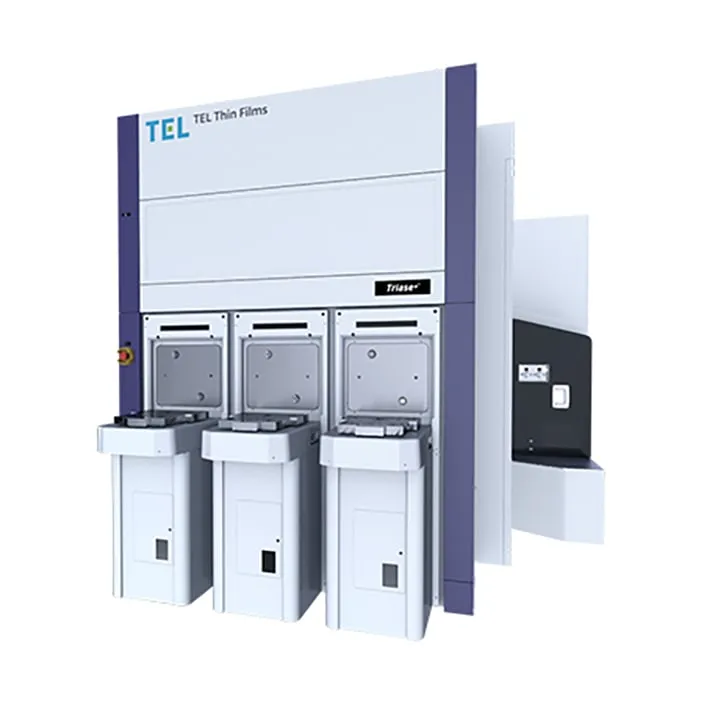
Architecture & Design
The TEL TRIAS SP's architecture is centered around its advanced etching technologies, which enable the precise control of pattern transfer processes. The tool's plasma reactive ion etching (RIE) capability allows for the etching of complex patterns on semiconductor wafers, while its chemical vapor deposition (CVD) system enables the deposition of thin films with high uniformity and conformality. The quartz boat, potentiostat, and power supply unit work in tandem to provide a stable and controlled environment for the etching and deposition processes.
The TEL TRIAS SP's design is focused on providing a high-degree of flexibility and customization, allowing users to tailor the tool to their specific fabrication needs. The tool's modular architecture enables the easy integration of new technologies and processes, making it an attractive solution for semiconductor manufacturers looking to stay at the forefront of technological advancements. Additionally, the TEL TRIAS SP's robotic repair system, offered by S3 Alliance, provides a quality repair solution for robotic systems, ensuring minimal downtime and maximizing productivity.
In terms of specific technical details, the TEL TRIAS SP features a plasma generation technology known as the Trias Slot Plane Antenna (SPA), which is targeted at nitridation of gate-dielectric films. This technology is essential for the fabrication of devices with 0.13-micron and below process technology nodes. While exact figures on the tool's process node capabilities were not publicly disclosed, it is clear that the TEL TRIAS SP is designed to support the fabrication of advanced semiconductor devices.
Performance & Thermal
The TEL TRIAS SP's performance is characterized by its ability to provide precise control over the pattern transfer process, enabling the fabrication of high-quality semiconductor devices. The tool's plasma reactive ion etching (RIE) and chemical vapor deposition (CVD) capabilities allow for the etching and deposition of complex patterns and thin films, respectively. While exact figures on the tool's throughput and yield were not publicly disclosed, it is clear that the TEL TRIAS SP is designed to provide high-performance and high-yield fabrication capabilities.
In terms of thermal management, the TEL TRIAS SP is designed to provide a stable and controlled environment for the etching and deposition processes. The tool's power supply unit and cooling system work in tandem to maintain a consistent temperature, minimizing the risk of thermal-related defects and ensuring optimal tool performance. While exact figures on the tool's thermal design power (TDP) were not publicly disclosed, it is clear that the TEL TRIAS SP is designed to provide efficient and effective thermal management.
Market Positioning
The TEL TRIAS SP is positioned as a high-end semiconductor fabrication tool, targeting advanced semiconductor manufacturers looking to fabricate devices with 0.13-micron and below process technology nodes. The tool's advanced etching technologies and customizable design make it an attractive solution for companies looking to stay at the forefront of technological advancements. Competitors in the market include other semiconductor fabrication tool manufacturers, such as Applied Materials and KLA-Tencor.
The TEL TRIAS SP's target buyer is likely to be a large semiconductor manufacturer with a significant budget for capital expenditures. The tool's high-performance and high-yield fabrication capabilities make it an attractive solution for companies looking to produce high-quality semiconductor devices. Additionally, the tool's customizable design and advanced etching technologies make it an attractive solution for companies looking to fabricate devices with complex patterns and thin films.
Verdict
In conclusion, the TEL TRIAS SP is a highly advanced semiconductor fabrication tool, featuring the latest etching technologies and customizable design. The tool's ability to provide precise control over the pattern transfer process, combined with its high-performance and high-yield fabrication capabilities, make it an attractive solution for advanced semiconductor manufacturers. While exact figures on the tool's performance and thermal management capabilities were not publicly disclosed, it is clear that the TEL TRIAS SP is designed to provide efficient and effective fabrication capabilities.
Pros of the TEL TRIAS SP include its advanced etching technologies, customizable design, and high-performance fabrication capabilities. Cons of the tool include its high cost and limited availability, as well as the need for significant expertise and resources to operate and maintain the tool. Overall, the TEL TRIAS SP is a highly advanced semiconductor fabrication tool, suitable for large semiconductor manufacturers looking to produce high-quality semiconductor devices.
Specifications
Technical Specifications
| Specification | Detail |
|---|---|
| Manufacturer | TEL |
| Model | Trias |
| Year | 2008 |
| Etching Technology | Plasma Reactive Ion Etching (RIE) and Chemical Vapor Deposition (CVD) |
| Process Node | 0.13-micron and below |
| Data Bus | Not publicly disclosed |
| Key ICs | Not publicly disclosed |
| TDP | Not publicly disclosed |
| Thermal Solution | Power supply unit and cooling system |
Frequently Asked Questions
Frequently Asked Questions
What is the TEL TRIAS SP's etching technology?
The TEL TRIAS SP features plasma reactive ion etching (RIE) and chemical vapor deposition (CVD) technologies.
What is the TEL TRIAS SP's process node capability?
The TEL TRIAS SP is capable of fabricating devices with 0.13-micron and below process technology nodes.
What is the TEL TRIAS SP's target market?
The TEL TRIAS SP is targeted at advanced semiconductor manufacturers looking to fabricate devices with complex patterns and thin films.