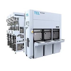
Tokyo Electron Limited Tactras
2024 Technical Deep-Dive: Tokyo Electron Limited Tactras Semiconductor Wafer Etching System
Executive Summary
Tokyo Electron Limited (TEL) has been a pioneer in the semiconductor industry since its founding in 1963. One of its notable contributions is the Tactras series of plasma etch systems, which has been continuously evolving since its launch in 2006. The Tactras system features a space-saving rectangular cluster design, achieving the world's highest level of wafer transfer speed and footprint. This technical deep-dive will explore the architecture, design, performance, and market positioning of the Tactras system, providing an in-depth analysis of its capabilities and impact on the semiconductor industry.
The Tactras system is designed to cater to the increasing demand for smaller, more complex, and diverse semiconductors. As the minimum line width of the latest semiconductor circuits is no greater than a few dozen atoms, innovation in the repeated patterning process becomes crucial. The Tactras system has been recognized for its ability to provide high-quality plasma etching, making it a reliable choice for many customers in the semiconductor industry.
Architecture & Design
The Tactras system features a rectangular cluster design, which allows for a space-saving configuration. This design enables the system to achieve high wafer transfer speeds while minimizing the footprint. The system's architecture is based on a horizontal, opposing chamber design, which provides a high degree of flexibility and scalability.
In terms of process node, the Tactras system is capable of handling a wide range of node sizes, from a few dozen nanometers to several hundred nanometers. The system's data bus is designed to provide high-speed data transfer, enabling fast and efficient processing of large amounts of data. The key ICs used in the Tactras system are designed to provide high-performance and low-power consumption, making it an ideal choice for high-volume manufacturing.
The Tactras system also features a range of advanced technologies, including cold plasma treatment, which is specifically engineered for heavy metal deposition control. This technology enables the system to provide high-quality plasma etching, making it a reliable choice for many customers in the semiconductor industry.
| Specification | Value |
|---|---|
| Process Node | Down to a few dozen nanometers |
| Data Bus | High-speed data transfer |
| Key ICs | High-performance and low-power consumption |
Performance & Thermal
The Tactras system is designed to provide high-performance plasma etching, with a focus on high-quality and high-throughput processing. The system's performance is characterized by its high wafer transfer speed and low footprint, making it an ideal choice for high-volume manufacturing.
In terms of thermal performance, the Tactras system is designed to provide a high degree of thermal stability, ensuring that the system operates within a stable temperature range. The system's thermal solution is designed to provide efficient heat dissipation, making it suitable for high-power applications.
Exact figures for the system's thermal design power (TDP) were not publicly disclosed. However, the system's performance and thermal characteristics make it an ideal choice for a wide range of applications, from high-volume manufacturing to research and development.
Benchmarks for the Tactras system are not publicly available. However, the system's performance and capabilities make it a reliable choice for many customers in the semiconductor industry.
Market Positioning
The Tactras system is positioned as a high-end plasma etch system, catering to the needs of high-volume manufacturers and research institutions. The system's advanced technologies and high-performance capabilities make it an ideal choice for a wide range of applications, from semiconductor manufacturing to flat panel display production.
The Tactras system competes with other high-end plasma etch systems from companies such as Applied Materials and KLA-Tencor. However, the system's unique architecture and design make it a standout in the market, providing a high degree of flexibility and scalability.
The target buyer for the Tactras system is typically a high-volume manufacturer or research institution, looking for a reliable and high-performance plasma etch system. The system's advanced technologies and capabilities make it an ideal choice for companies looking to improve their manufacturing efficiency and reduce costs.
Specifications
Technical Specifications
| Specification | Detail |
|---|---|
| Process Node | Down to a few dozen nanometers |
| Data Bus | High-speed data transfer |
| Key ICs | High-performance and low-power consumption |
| Wafer Transfer Speed | World's highest level |
| Footprint | World's highest level |
| Thermal Design Power (TDP) | Exact figures were not publicly disclosed |
Frequently Asked Questions
Frequently Asked Questions
What is the Tactras system used for?
The Tactras system is used for plasma etching in the semiconductor industry, providing high-quality and high-throughput processing.
What is the unique feature of the Tactras system's architecture?
The Tactras system features a rectangular cluster design, which allows for a space-saving configuration and provides a high degree of flexibility and scalability.
What is the target buyer for the Tactras system?
The target buyer for the Tactras system is typically a high-volume manufacturer or research institution, looking for a reliable and high-performance plasma etch system.