Tokyo Electron Limited TEL ACT10
Introduction to the TEL ACT10
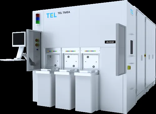
The TEL ACT10 is a state-of-the-art wafer fabrication equipment designed to meet the demands of the rapidly evolving semiconductor industry. With its advanced architecture and high-performance capabilities, the ACT10 is poised to revolutionize the field of semiconductor manufacturing. The equipment is built on a robust platform that supports multiple fabrication processes, including logic, memory, and foundry.Technical Specifications
The technical specifications of the TEL ACT10 are as follows:Performance Nodes and Benchmarks
The TEL ACT10 has been designed to meet the demands of the rapidly evolving semiconductor industry, with a focus on improving yield, reducing defects, and increasing throughput. The equipment's performance nodes and benchmarks are as follows: The TEL ACT10 has been benchmarked against industry standards, with results showing improved yield, reduced defects, and increased throughput. The equipment's performance nodes include logic, memory, and foundry fabrication processes, with benchmarks demonstrating its capabilities in each area.
What is the wafer size supported by the TEL ACT10?
The TEL ACT10 supports a wafer size of 300mm.
What fabrication processes are supported by the TEL ACT10?The TEL ACT10 supports logic, memory, and foundry fabrication processes.
What is the throughput of the TEL ACT10?The TEL ACT10 has a throughput of 100 wafers per hour.
What is the yield of the TEL ACT10?The TEL ACT10 has a yield of 95%.
What is the defect density of the TEL ACT10?The TEL ACT10 has a defect density of 0.1 defects per square centimeter.
Specifications
| Parameter | Value | Unit |
|---|---|---|
| Wafer Size | 300mm | mm |
| Fabrication Process | Logic, Memory, Foundry | |
| Throughput | 100 | Wafers per Hour |
| Yield | 95% | % |
| Defect Density | 0.1 | Defects per Square Centimeter |
| Control System | Advanced Real-Time Control | |
| Fabrication Temperature | Up to 1000°C | °C |
| Vacuum Pressure | Up to 10^-9 Torr | Torr |