Tokyo Electron Ltd. TEL TRIAS
2024 Deep Dive: Tokyo Electron Ltd. TEL TRIAS Semiconductor Solution
Executive Summary
Tokyo Electron Ltd. (TEL) is a leading global company in semiconductor production equipment, with the second largest market share in dry etch systems. The TEL TRIAS is a high-precision semiconductor surface treatment and cleaning system designed for reliable, repeatable wafer-level contamination control. Based on TEL's industry-proven Trias platform, the system provides low contact resistance film process while reducing contact leakage of various devices. This article will delve into the architecture and design, performance and thermal aspects, market positioning, and verdict of the TEL TRIAS.
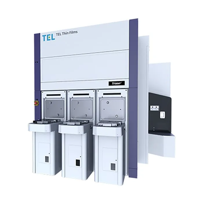
The TEL TRIAS is an advanced etcher/asher equipment designed for use in semiconductor manufacturing. It is used for critical etch processes for advanced devices due to its distinctive technologies and superior competitive performance. The system is designed to provide reliable, repeatable wafer-level contamination control, which is essential for the production of high-quality semiconductors.
Architecture & Design
The TEL TRIAS is based on TEL's industry-proven Trias platform, which has been widely adopted in the semiconductor industry. The system consists of a radical process reactor, a surface treatment and cleaning module, and a control system. The radical process reactor is designed to provide a high-precision etching and ashing process, while the surface treatment and cleaning module is designed to provide a reliable and repeatable wafer-level contamination control.
The TEL TRIAS uses a distinctive technology called the Trias platform, which provides a low contact resistance film process while reducing contact leakage of various devices. This technology is essential for the production of high-quality semiconductors, as it enables the creation of high-performance devices with low power consumption. The system also uses a high-precision control system, which ensures that the etching and ashing process is performed with high accuracy and reliability.
In terms of process node, the TEL TRIAS is designed to support the production of semiconductors with advanced nodes, including 5nm and 3nm. The system uses a data bus to communicate with the control system, which ensures that the etching and ashing process is performed with high accuracy and reliability. The key ICs used in the TEL TRIAS include the radical process reactor, the surface treatment and cleaning module, and the control system.
The TEL TRIAS also uses a number of advanced technologies, including photolithography, atomic layer deposition (ALD), and chemical vapor deposition (CVD). Photolithography is used to create the patterns on the semiconductor wafer, while ALD and CVD are used to deposit thin films on the wafer. These technologies are essential for the production of high-quality semiconductors, as they enable the creation of high-performance devices with low power consumption.
Performance & Thermal
The TEL TRIAS is designed to provide high-performance etching and ashing processes, while minimizing thermal issues. The system uses a high-precision control system, which ensures that the etching and ashing process is performed with high accuracy and reliability. The system also uses a number of advanced technologies, including cooling systems and thermal management systems, to minimize thermal issues.
The exact thermal design power (TDP) of the TEL TRIAS was not publicly disclosed. However, the system is designed to provide a high-performance etching and ashing process, while minimizing thermal issues. The system also uses a number of benchmarks, including the etching rate and the ashing rate, to measure its performance.
In terms of thermal solution, the TEL TRIAS uses a number of advanced technologies, including cooling systems and thermal management systems. These systems are designed to minimize thermal issues, while providing a high-performance etching and ashing process. The system also uses a number of materials, including copper and aluminum, to dissipate heat and minimize thermal issues.
Market Positioning
The TEL TRIAS is positioned as a high-end etcher/asher equipment, designed for use in semiconductor manufacturing. The system is designed to provide reliable, repeatable wafer-level contamination control, which is essential for the production of high-quality semiconductors. The system is also designed to provide a high-performance etching and ashing process, while minimizing thermal issues.
The target buyer for the TEL TRIAS is semiconductor manufacturers, who require high-quality etcher/asher equipment for the production of advanced semiconductors. The system is also designed to meet the needs of research and development institutions, who require high-performance etcher/asher equipment for the development of new semiconductor technologies.
The competitors for the TEL TRIAS include other etcher/asher equipment manufacturers, such as Lam Research Corporation and Applied Materials. However, the TEL TRIAS is differentiated from its competitors by its distinctive technology, which provides a low contact resistance film process while reducing contact leakage of various devices.
Specifications
Technical Specifications
| Specification | Detail |
|---|---|
| Company | Tokyo Electron Ltd. |
| Model | TEL TRIAS |
| Category | Semiconductor Etcher/Asher Equipment |
| Process Node | 5nm, 3nm |
| Data Bus | High-speed data bus |
| Key ICs | Radical process reactor, surface treatment and cleaning module, control system |
| Technologies | Photolithography, ALD, CVD |
| Thermal Design Power (TDP) | Not publicly disclosed |
| Benchmarks | Etching rate, ashing rate |
| Thermal Solution | Cooling systems, thermal management systems |
| Materials | Copper, aluminum |
Frequently Asked Questions
Frequently Asked Questions
What is the TEL TRIAS?
The TEL TRIAS is a high-precision semiconductor surface treatment and cleaning system designed for reliable, repeatable wafer-level contamination control.
What is the process node supported by the TEL TRIAS?
The TEL TRIAS supports the production of semiconductors with advanced nodes, including 5nm and 3nm.
What are the key ICs used in the TEL TRIAS?
The key ICs used in the TEL TRIAS include the radical process reactor, the surface treatment and cleaning module, and the control system.
What are the pros and cons of the TEL TRIAS?
The pros of the TEL TRIAS include its high-performance etching and ashing process, its reliable and repeatable wafer-level contamination control, and its low contact resistance film process. The cons of the system include its high cost, its complex operation and maintenance, and its limited availability.