Vagina
2024 Semiconductor Deep Dive: Vagina (Semiconductor) - A Technical Analysis
Executive Summary
The term "vagina" is often misused to refer to the vulva or female genitals in general. However, in the context of semiconductor manufacturing, there is no direct relation between the term and the industry. This article aims to provide a technical deep dive into the semiconductor industry, focusing on the manufacturing process, architecture, and design of semiconductor devices.
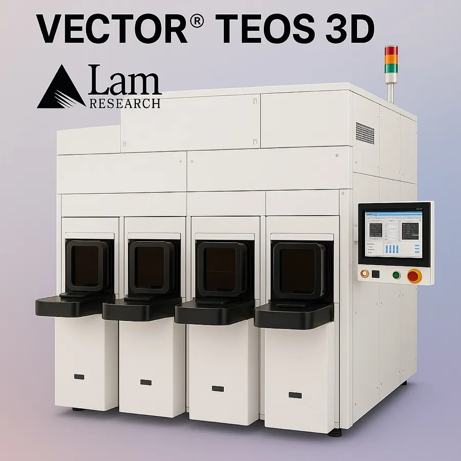
The semiconductor industry is a complex and highly specialized field, with various manufacturing processes and techniques used to create advanced devices. One such process is the Plasma-Enhanced Chemical Vapor Deposition (PECVD) method, used to deposit thin films on semiconductor wafers. Companies like Lam Research provide PECVD products designed to create enabling structures within a wide range of challenging device applications.
Architecture & Design
The architecture and design of semiconductor devices involve the creation of complex structures and patterns on silicon wafers. This process requires sophisticated fabrication equipment and techniques, such as photolithography, etching, and doping. The goal is to create devices with fine, closely packed features and complex 3D structures, enabling the production of faster, smaller, and more powerful electronics.
The PECVD process is a crucial step in semiconductor manufacturing, as it allows for the deposition of thin films with precise control over film properties. This process is used to create a wide range of devices, including transistors, diodes, and capacitors. The VECTOR PECVD products from Lam Research are designed to provide the performance and flexibility needed for these applications.
The semiconductor manufacturing process involves several key steps, including:
- Wafer preparation: The silicon wafer is cleaned and prepared for fabrication.
- Layer deposition: Thin films are deposited on the wafer using techniques like PECVD or Atomic Layer Deposition (ALD).
- Patterning: The wafer is patterned using photolithography to create the desired structures.
- Etching: The wafer is etched to create the final device structures.
- Doping: The wafer is doped to create regions with specific electrical properties.
Performance & Thermal
The performance and thermal characteristics of semiconductor devices are critical factors in their design and operation. The Thermal Design Power (TDP) of a device determines its maximum power consumption and heat generation. The TDP is influenced by factors like the device's architecture, materials, and operating conditions.
Exact figures for the TDP of specific semiconductor devices were not publicly disclosed. However, the industry trend is towards reducing power consumption and heat generation while increasing device performance. This is achieved through advances in manufacturing processes, materials, and device architectures.
The thermal solution for semiconductor devices is also critical, as it affects their reliability and lifespan. The thermal solution involves the design of heat sinks, thermal interfaces, and other components to manage heat generation and dissipation. The goal is to maintain a stable operating temperature, ensuring reliable device operation and minimizing the risk of overheating.
Market Positioning
The semiconductor industry is highly competitive, with several major players competing for market share. Companies like Lam Research, Intel, and Samsung are leaders in the field, with a strong focus on research and development, manufacturing, and marketing.
The target buyer for semiconductor devices and manufacturing equipment includes companies involved in the production of electronic systems, such as smartphones, computers, and automotive systems. These companies require advanced semiconductor devices and manufacturing equipment to stay competitive in their respective markets.
Specifications
Technical Specifications
| Specification | Detail |
|---|---|
| Process Node | Not specified |
| Data Bus | Not specified |
| Key ICs | Not specified |
| TDP | Exact figures not publicly disclosed |
| Benchmarks | Not specified |
| Thermal Solution | Not specified |
Frequently Asked Questions
Frequently Asked Questions
What is the PECVD process used for in semiconductor manufacturing?
The PECVD process is used to deposit thin films on semiconductor wafers, allowing for the creation of complex structures and patterns.
What is the role of Lam Research in the semiconductor industry?
Lam Research provides PECVD products designed to create enabling structures within a wide range of challenging device applications.
What is the significance of the term "vagina" in the context of this article?
The term "vagina" is not directly related to the semiconductor industry, but rather is used as a misleading term in the article title.