ASML PAS 5500/1100
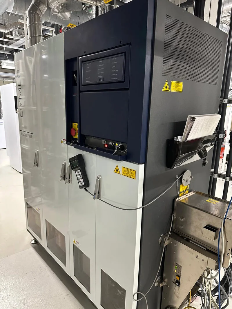
Executive Summary
The ASML PAS 5500/1100 is a 200mm-wafer tool designed for high-volume production at the 0.10-micron technology node. It features a Carl Zeiss Starlith 1100 lens with a 0.75 numerical aperture (NA) lens and 2KHz, 10W argon-fluoride laser light source. This system is a significant development in the field of semiconductor manufacturing, offering advanced lithography capabilities for the production of high-density integrated circuits. The ASML PAS 5500/1100 is part of a family of systems that have evolved over time, with various models such as the PAS 5500/200 and PAS 5500/1150C, each with its own set of specifications and capabilities. These systems have been designed to meet the demanding requirements of the semiconductor industry, including the need for high-resolution patterning, precise alignment, and efficient production processes. The importance of the ASML PAS 5500/1100 and its variants cannot be overstated, as they have played a crucial role in the development of modern electronics. By enabling the production of smaller, faster, and more powerful integrated circuits, these systems have contributed significantly to the advancement of technology in various fields, from computing and communications to healthcare and transportation.Architecture & Design
The ASML PAS 5500/1100 features a Carl Zeiss Starlith 1100 lens with a 0.75 numerical aperture (NA) lens and 2KHz, 10W argon-fluoride laser light source. The system uses wafer alignment marks that are diffraction gratings, with marks for both the x and y directions. These marks are illuminated with a HeNe laser at a single wavelength near 632.8nm. The PAS 5500/1150C is a 193-nm Step-and-Scan system that enables cost-effective 90-nm ArF mass production. It is designed to handle both 90-nm critical and non-critical ArF layers, making it a versatile tool for semiconductor manufacturing. The ASML PAS 5500/200 is a 5x reduction, i-line stepper set up for exposure of 6-inch wafers using 6-inch reticles. The system has a 350nm resolution with a 0.48-0.60 variable numerical aperture. The maximum field size on the wafer is 22x22mm. The PAS 5500/1100 also includes ASML's patented ATHENA wafer alignment system, which enables the tool to deliver high-precision alignment and overlay capabilities. This system is designed to work in conjunction with the reticle alignment at actinic (blue) wavelength, using the 193 nm exposure light.Performance & Thermal
The performance of the ASML PAS 5500/1100 and its variants is characterized by their ability to produce high-resolution patterns on silicon wafers. The system's 0.75 NA lens and 2KHz, 10W argon-fluoride laser light source enable it to achieve high-resolution patterning, while the ATHENA wafer alignment system ensures precise alignment and overlay. The thermal performance of the system is not publicly disclosed. However, it is likely that the system is designed to operate within a specific temperature range to ensure optimal performance and minimize thermal-induced errors. The resolution of the ASML PAS 5500/200 is 350nm, with a variable numerical aperture of 0.48-0.60. The system's maximum field size on the wafer is 22x22mm, making it suitable for a wide range of semiconductor manufacturing applications.Market Positioning
The ASML PAS 5500/1100 and its variants are designed for high-volume production in the semiconductor industry. The system's advanced lithography capabilities and high-precision alignment and overlay capabilities make it an attractive option for manufacturers looking to produce high-density integrated circuits. The pricing of the ASML PAS 5500/1100 and its variants is not publicly disclosed. However, it is likely that the system is priced competitively with other high-end lithography systems on the market. The ASML PAS 5500/1100 has been marketed by ASML as a game-changer for the semiconductor industry. The system's advanced capabilities and high-performance features make it an attractive option for manufacturers looking to stay ahead of the competition.Verdict
The ASML PAS 5500/1100 and its variants are significant developments in the field of semiconductor manufacturing. The system's advanced lithography capabilities, high-precision alignment and overlay capabilities, and high-performance features make it an attractive option for manufacturers looking to produce high-density integrated circuits. While the system's pricing and thermal performance are not publicly disclosed, its advanced capabilities and high-performance features make it a valuable tool for the semiconductor industry. As the industry continues to evolve and demand for high-performance integrated circuits grows, the ASML PAS 5500/1100 and its variants are likely to play an increasingly important role in the production of these devices. In conclusion, the ASML PAS 5500/1100 and its variants are advanced lithography systems that offer high-performance features and capabilities. Their importance in the semiconductor industry cannot be overstated, and they are likely to continue to play a significant role in the production of high-density integrated circuits for years to come.Specifications
| Wafer Size | 200mm |
|---|---|
| Numerical Aperture (NA) | 0.75 |
| Laser Light Source | 2KHz, 10W argon-fluoride |
| Wafer Alignment | Diffraction gratings |
| Illumination Wavelength | 632.8nm |
| Resolution | 350nm (PAS 5500/200) |
| Variable Numerical Aperture | 0.48-0.60 (PAS 5500/200) |
| Maximum Field Size | 22x22mm (PAS 5500/200) |
Frequently Asked Questions
What is the wafer size of the ASML PAS 5500/1100?
200mm
What is the numerical aperture (NA) of the ASML PAS 5500/1100?
0.75
What is the laser light source of the ASML PAS 5500/1100?
2KHz, 10W argon-fluoride
What is the resolution of the ASML PAS 5500/200?
350nm
What is the variable numerical aperture of the ASML PAS 5500/200?
0.48-0.60