Extreme ultraviolet lithography
Executive Summary
Extreme ultraviolet lithography (EUVL) is a technology used in the semiconductor industry for manufacturing integrated circuits (ICs). It utilizes 13.5 nm extreme ultraviolet (EUV) light from a laser-pulsed tin (Sn) plasma to create intricate patterns on semiconductor substrates. As of 2025, ASML Holding is the only company that produces and sells EUV systems for chip production, targeting 5 nanometer (nm) and 3 nm process nodes. The history of EUVL dates back to the 1960s when visible light was used for the production of integrated circuits. Over the years, the industry transitioned to ultraviolet (UV) light, with wavelengths as short as 365 nm, and then to deep UV with wavelengths of 248 nm and 193 nm. The next step was the development of EUV, which uses wavelengths near 13.5 nm. However, EUV light is absorbed by glass and air, requiring the use of mirrors in vacuum instead of lenses to focus the beams of light.Architecture & Design
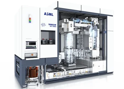
EUVL is a type of photolithography that uses a laser-pulsed tin droplet plasma to produce a pattern by using a reflective photomask to expose a substrate covered by photoresist. The EUV wavelengths used in EUVL are near 13.5 nanometers (nm), with tin ions in the ionic states from Sn IX to Sn XIV giving photon emission spectral peaks around 13.5 nm from 4p64dn – 4p54dn+1 + 4dn−14f ionic state transitions. The development of EUVL was first proposed by engineer Hiroo Kinoshita in the mid-1980s while working at Nippon Telegraph and Telephone (NTT) in Japan. Kinoshita successfully demonstrated the first EUV images at a 1986 Japan Society of Applied Physics (JSAP) meeting. Despite initial skepticism, Kinoshita continued EUV research at NTT and organized joint research with other companies. ASML Holding, a leading manufacturer of semiconductor equipment, has been at the forefront of EUVL development. The company's EUV systems are designed to produce features down to 5 nm and 3 nm at high volumes. ASML's TWINSCAN NXT:1950i system, for example, uses a water immersion lens and an argon fluoride laser that produces light at a wavelength of 193 nm to produce features down to 32 nanometres at up to 200 wafers per hour.Performance & Thermal
The performance of EUVL systems is not publicly disclosed in terms of specific benchmarks or thermal design power (TDP). However, it is known that EUVL systems are designed to produce high-quality patterns on semiconductor substrates with high throughput. The use of EUV light allows for the creation of smaller features, which is essential for the production of advanced semiconductor devices. The thermal management of EUVL systems is critical due to the high energy density of the EUV light. The systems are designed to operate in a vacuum environment, which helps to reduce thermal losses and maintain a stable temperature. However, the exact thermal performance of EUVL systems is not publicly disclosed.Market Positioning
ASML Holding is the only company that produces and sells EUV systems for chip production as of 2025. The company's EUV systems are designed to target 5 nm and 3 nm process nodes, which are the most advanced nodes in the semiconductor industry. The market for EUVL systems is highly competitive, with other companies such as Canon and Nikon having previously developed EUVL technology but stopping development due to technical challenges. The pricing of EUVL systems is not publicly disclosed. However, it is known that the development and production of EUVL systems require significant investment in research and development, manufacturing, and testing. The cost of EUVL systems is likely to be high due to the complexity of the technology and the limited demand for these systems.Verdict
In conclusion, EUVL is a critical technology for the production of advanced semiconductor devices. The use of EUV light allows for the creation of smaller features, which is essential for the production of high-performance devices. ASML Holding is the only company that produces and sells EUV systems for chip production, targeting 5 nm and 3 nm process nodes. While the performance and thermal characteristics of EUVL systems are not publicly disclosed, it is clear that these systems play a vital role in the production of advanced semiconductor devices. The development of EUVL has been a long and challenging process, with significant investment in research and development required to overcome technical challenges. The market for EUVL systems is highly competitive, with other companies having previously developed EUVL technology but stopping development due to technical challenges. However, ASML Holding has emerged as the leader in EUVL technology, with its systems being used by major semiconductor manufacturers worldwide. In the future, EUVL is expected to continue playing a critical role in the production of advanced semiconductor devices. The development of new EUVL technologies, such as high-numerical-aperture (high-NA) EUVL, is expected to further improve the resolution and throughput of EUVL systems. As the semiconductor industry continues to evolve, EUVL is likely to remain a key technology for the production of high-performance devices. The history of EUVL is a testament to the power of innovation and perseverance in the face of technical challenges. From its humble beginnings in the 1960s to the present day, EUVL has come a long way, with significant advances in technology and manufacturing. As the semiconductor industry continues to push the boundaries of what is possible, EUVL is likely to remain at the forefront of this effort, enabling the production of smaller, faster, and more powerful devices. In addition to its technical challenges, EUVL also faces significant economic and environmental challenges. The production of EUVL systems requires significant investment in research and development, manufacturing, and testing, which can be costly and time-consuming. Furthermore, the use of EUV light requires the use of complex and expensive optics, which can be difficult to manufacture and maintain. Despite these challenges, EUVL remains a critical technology for the production of advanced semiconductor devices. Its ability to create smaller features and higher-resolution patterns makes it an essential tool for the semiconductor industry. As the industry continues to evolve, EUVL is likely to remain a key technology, enabling the production of smaller, faster, and more powerful devices. In conclusion, EUVL is a complex and challenging technology that has come a long way since its inception in the 1960s. From its humble beginnings to the present day, EUVL has evolved significantly, with significant advances in technology and manufacturing. As the semiconductor industry continues to push the boundaries of what is possible, EUVL is likely to remain at the forefront of this effort, enabling the production of smaller, faster, and more powerful devices. The future of EUVL is bright, with significant advances in technology and manufacturing expected in the coming years. The development of new EUVL technologies, such as high-NA EUVL, is expected to further improve the resolution and throughput of EUVL systems. As the semiconductor industry continues to evolve, EUVL is likely to remain a key technology, enabling the production of smaller, faster, and more powerful devices. In the end, EUVL is a testament to the power of innovation and perseverance in the face of technical challenges. Its ability to create smaller features and higher-resolution patterns makes it an essential tool for the semiconductor industry. As the industry continues to push the boundaries of what is possible, EUVL is likely to remain at the forefront of this effort, enabling the production of smaller, faster, and more powerful devices.Specifications
| Wavelength | 13.5 nm |
|---|---|
| Process Node | 5 nm and 3 nm |
| Company | ASML Holding |
| Technology | Photolithography |
| Light Source | Laser-pulsed tin droplet plasma |
| Ionic States | Sn IX to Sn XIV |
| Photon Emission Spectral Peaks | 4p64dn – 4p54dn+1 + 4dn−14f ionic state transitions |
Frequently Asked Questions
What is Extreme Ultraviolet Lithography (EUVL)?
EUVL is a technology used in the semiconductor industry for manufacturing integrated circuits (ICs) that utilizes 13.5 nm extreme ultraviolet (EUV) light from a laser-pulsed tin (Sn) plasma to create intricate patterns on semiconductor substrates.
Who is the only company that produces and sells EUV systems for chip production as of 2025?
ASML Holding
What are the process nodes targeted by ASML's EUV systems?
5 nm and 3 nm
What is the wavelength of the EUV light used in EUVL?
13.5 nm
What is the light source used in EUVL?
Laser-pulsed tin droplet plasma